
Request Vertical GaN Wafers
UniversityWafer supplies vertical gallium nitride wafers and custom GaN epitaxial structures for high-voltage power device research. Vertical GaN is used in next-generation power devices, vertical MOSFETs, Schottky diodes, and wide-bandgap semiconductor applications.
We can help source bulk GaN substrates, n-type drift layers, vertical MOSFET epitaxy, diode structures, and SBD structures for research and limited production.
Get Your Vertical GaN Wafer Quote FAST! Or, Buy Online and Start Researching Today!
Vertical GaN Wafer Options
- Bulk GaN substrates
- n-type GaN drift layers
- Vertical MOSFET epitaxial structures
- Schottky diode and SBD stacks
- Research-grade and production-grade material
Vertical GaN FAQs
What makes Vertical GaN different?
Vertical GaN conducts current through the GaN wafer thickness, enabling higher voltage and lower resistance than many lateral GaN designs.
What substrates does Vertical GaN require?
Vertical GaN devices typically require low-defect bulk GaN substrates and carefully controlled epitaxial drift layers.
What applications use Vertical GaN?
Vertical GaN is used for EV power electronics, solar inverters, data centers, industrial drives, grid infrastructure, and high-voltage power conversion.
What Is Vertical Gallium Nitride?
Vertical Gallium Nitride (Vertical GaN) is an advanced wide-bandgap semiconductor technology designed for next-generation high-power electronic devices. Unlike conventional lateral GaN devices, where current flows across the wafer surface, vertical GaN devices conduct current through the thickness of the wafer. This architecture enables higher voltage capability, greater current density, and improved thermal performance.
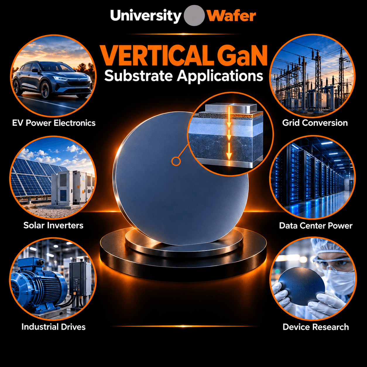
Vertical GaN is being developed for electric vehicles, renewable energy systems, industrial automation, data centers, and smart grid infrastructure because it combines the excellent electrical properties of GaN with a device structure optimized for high-voltage operation.
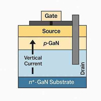
How Vertical GaN Works
A vertical GaN device conducts electrons through a thick n-type drift layer grown on a low-defect bulk GaN substrate. Since current flows vertically rather than laterally, the active device area can support much higher blocking voltages while maintaining low on-resistance. This makes Vertical GaN particularly attractive for applications requiring both high efficiency and compact device size.
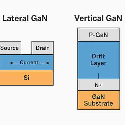
Advantages of Vertical GaN
- Higher blocking voltage than conventional lateral GaN devices.
- Lower specific on-resistance (RDS(on)) for improved efficiency.
- Excellent thermal performance for demanding power applications.
- High switching frequency to reduce passive component size.
- Improved scalability for high-current power electronics.
- Suitable for 1.2 kV to 10 kV-class power devices.
Available Vertical GaN Materials
UniversityWafer supplies materials for vertical power device development, including research-grade and production-grade bulk GaN substrates, custom epitaxial structures, drift layers, and device-ready wafers for advanced semiconductor research.
| Specification | Typical Offering |
|---|---|
| Wafer Diameter | 2", 4", and 6" Bulk GaN |
| Substrate Type | Low-defect Bulk GaN |
| Drift Layer | Custom n-type epitaxy |
| Device Structures | Vertical MOSFETs, Schottky Diodes, SBDs |
| Voltage Class | 1.2–10 kV |
| Surface Finish | Double-side polished and epi-ready options |
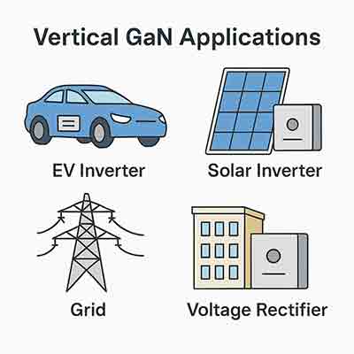
Applications of Vertical GaN
Vertical GaN technology is expected to transform high-power electronics by delivering higher efficiency, faster switching, and lower system losses. Common research and commercial applications include:
- Electric vehicle traction inverters
- Solar power inverters
- Grid-scale power conversion
- Industrial motor drives
- High-efficiency data center power supplies
- Renewable energy storage systems
- Advanced aerospace and defense electronics
Why Choose UniversityWafer?
- Research-grade and production-quality bulk GaN wafers
- Custom vertical MOSFET and Schottky diode epitaxial structures
- Low-defect GaN substrates optimized for high-voltage devices
- Fast quotations for universities, national laboratories, and commercial R&D
- Worldwide shipping and technical support
Related Vertical GaN Resources
- Bulk Gallium Nitride (GaN) Wafers
- Gallium Nitride Semiconductor
- GaN on Sapphire
- Gallium Nitride (GaN) Wafers
- GaN HEMT Wafers
- Silicon Carbide (SiC) Wafers
- Power Semiconductor Devices
- MOSFET Research
- Schottky Barrier Diode (SBD) Structures
- Semiconductor Device Fabrication
- Semiconductor Epitaxial Wafers
- Wide-Bandgap Semiconductors
- Solar Power Applications
- Advanced Semiconductor Research