
GaN Wafers for Semiconductor Research
UniversityWafer supplies gallium nitride material platforms for university and commercial research. Options include GaN epitaxial wafers on sapphire and AlGaN/GaN heterostructures. Confirm the substrate, layer stack and required characterization when requesting a quote.
A GaN template or research wafer is a starting material for device fabrication. It should not be assumed to include finished transistors, contacts or a complete LED structure.
Get Your Quote Fast! Or Buy GaN on Sapphire Wafers Online and start researching today!
Which GaN Wafer Specifications Should You Request?
- Base substrate: Specify sapphire, SiC, silicon or bulk GaN, according to the process.
- Size and thickness: Include wafer diameter or sample dimensions, substrate thickness and tolerances.
- Epitaxial stack: State GaN thickness and any buffer, barrier, cap or active layers needed for the device.
- Electrical properties: Include doping type, carrier concentration, resistivity or sheet resistance when required.
- Crystal and surface: Specify orientation, polarity, miscut, polish, roughness and acceptable defect limits.
- Process needs: Describe the intended device, processing temperatures, quantity and characterization requirements.
For HEMT research, a GaN layer alone may not provide the desired transistor structure. Specify the AlGaN barrier and GaN channel along with buffer layers and the base substrate.
What Is Gallium Nitride?
Gallium nitride (GaN) is a III-V compound semiconductor made from gallium and nitrogen. Its direct bandgap is approximately 3.4 eV at room temperature. The wide bandgap and high breakdown-field capability make it useful for electronic devices, while the direct bandgap supports light-emitting structures.
GaN device layers can be grown on other materials or on bulk GaN. The semiconductor substrate and epitaxial design influence crystal quality, electrical isolation, thermal behavior and the fabrication route.
GaN Semiconductor Device Applications
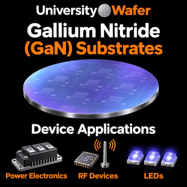
Power Electronics and Fast-Switching Transistors
GaN power transistors are used in compact chargers, adapters, server power supplies and power-conversion systems. Fast switching can reduce switching losses and allow smaller passive components in suitable circuit designs. Device ratings, gate drive, layout and cooling determine the result.
For application background, see Texas Instruments' GaN power technology overview. Researchers developing devices can review field-effect transistor substrates and specify the required epitaxial structure separately.
RF and Microwave Devices
GaN high-electron-mobility transistors (HEMTs) support RF power amplifier research for wireless infrastructure, radar and microwave systems. AlGaN/GaN heterostructures combine layers with different properties to form the transistor platform. Substrate losses, heat removal and epitaxial quality matter in high-frequency designs.
LEDs, Laser Diodes and Optical Devices
GaN-based material systems support blue and violet emitters, laser diodes and optical research. InGaN alloys are important in many blue and green LEDs, while aluminum-containing AlGaN materials extend the nitride system toward shorter ultraviolet wavelengths. The active-layer composition determines the emission range; a generic GaN wafer is not interchangeable with every LED structure.
The U.S. Department of Energy's UV LED benchmark report explains the relevant nitride alloy system. Nanopatterned emitters and optical devices may also require nanostructure fabrication substrates.
Compare GaN Substrate Platforms
| Platform | Common research use | Selection considerations |
|---|---|---|
| GaN on sapphire | Optoelectronic devices and nitride templates | Orientation, layer thickness, defect requirements and heat-removal path |
| GaN on SiC | RF and high-power device structures | SiC electrical type, epitaxial stack and thermal interfaces |
| GaN on silicon | Power-device research | Buffer design, stress, bow and tool-compatible wafer size |
| Bulk or freestanding GaN | Homoepitaxial growth and device development | Polarity, orientation, doping, defect limits and surface preparation |
Sapphire, SiC and silicon are different base materials. None substitutes for the GaN device layer itself. Confirm availability for the exact wafer and layer specification.
GaN vs. SiC and Silicon
GaN and silicon carbide are distinct wide-bandgap semiconductors. GaN is used in fast-switching power devices, RF electronics and emitters; SiC is used in high-voltage power devices and can also support GaN epitaxy. Conventional silicon remains widely used across electronics.
Choose the material from the required voltage, frequency, losses, thermal design, fabrication process and cost constraints. GaN is not automatically the lowest-cost or best-performing choice for every device. See SiC substrate applications for the related material platform.
Gallium Nitride Semiconductor FAQs
Is GaN the same as GaN on sapphire?
GaN names the semiconductor material. GaN on sapphire describes a layered wafer with GaN grown on a sapphire base. Bulk GaN, GaN on silicon and GaN on SiC are other configurations.
What is the difference between a GaN template and a HEMT wafer?
A template provides a foundation for further processing or growth. A HEMT wafer requires the specific heterostructure needed for the transistor design. Request the layer sequence and electrical specifications rather than assuming a generic template is device-ready.
Are all GaN-based LEDs ultraviolet LEDs?
No. Nitride emitters span different wavelengths according to alloy composition and device design. Specify the required wavelength and active-layer structure when sourcing material for optical devices.
What should I include in a GaN wafer quote?
Include substrate material, wafer size, orientation, layer thicknesses, doping, surface quality, quantity and intended application. Request a gallium nitride substrate quote to discuss the required stack.