
What Is a MOSFET?
A MOSFET (metal-oxide-semiconductor field-effect transistor) is a voltage-controlled semiconductor device used to switch or control electrical current. MOSFETs are fundamental components in modern integrated circuits and are also widely used as discrete devices in power electronics, motor control, power conversion, and other electronic systems.
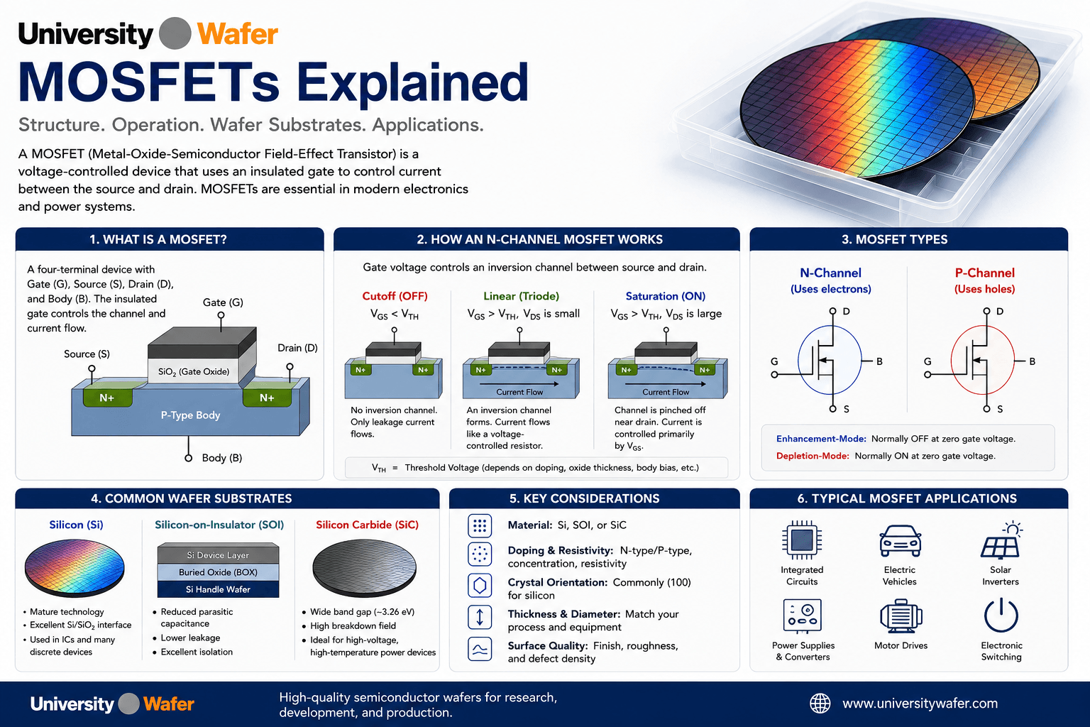
A MOSFET is fundamentally a four-terminal device consisting of the gate, source, drain, and body (also called the bulk or substrate terminal). In many discrete MOSFETs, the body is internally connected to the source, so the packaged component is commonly treated as a three-terminal device.
The defining feature of a MOSFET is its electrically insulated gate. A voltage applied between the gate and source produces an electric field that changes the carrier distribution near the semiconductor surface. This electrostatic control can create or modify a conductive channel between the source and drain.
What Are the Main Parts of a MOSFET?
Understanding the physical structure of a MOSFET helps explain how the device controls electrical current. Its principal regions are:
- Gate: A conductive electrode used to control the electrical state of the channel.
- Gate dielectric: An electrically insulating layer separating the gate electrode from the semiconductor. Silicon dioxide (SiO2) has historically been widely used, while modern MOS technologies may use other dielectric materials, including high-k dielectrics.
- Source: One terminal connected to the channel through which charge carriers enter or leave the active region, depending on device type and bias conditions.
- Drain: The other terminal connected to the channel. Current flows through the channel between the source and drain when the device is appropriately biased.
- Body or bulk: The semiconductor region in which the MOSFET structure is formed. Its electrical potential can influence threshold voltage and device behavior.
- Channel: The electrically controlled region near the semiconductor-dielectric interface that provides a conduction path between source and drain when the MOSFET is turned on.
How Does a MOSFET Work?
A MOSFET controls current by using an electric field generated by the gate voltage. Because the gate is separated from the semiconductor by an insulating dielectric, ideally there is no steady DC conduction current through the gate dielectric. Real devices do, however, exhibit finite leakage, and current is required to charge and discharge the gate capacitance during switching.
Consider a conventional n-channel enhancement-mode MOSFET (NMOS) formed using n-type source and drain regions in a p-type body. When the gate-to-source voltage is sufficiently positive, the electric field produced by the gate changes the carrier distribution beneath the gate.
As the gate voltage increases, holes are depleted from the semiconductor surface and electrons accumulate near the semiconductor-dielectric interface. When sufficient inversion occurs, an electron inversion channel connects the source and drain. Applying a drain-to-source voltage can then produce current through this channel.
The gate therefore controls the conductivity of the channel electrostatically rather than by directly injecting current through the gate dielectric.
What Is MOSFET Threshold Voltage?
The threshold voltage (VTH) is an important MOSFET parameter associated with the gate voltage at which significant channel inversion begins according to a specified device definition or measurement criterion.
Threshold voltage is not a universal constant for all MOSFETs. It depends on device structure and material properties, including factors such as:
- Semiconductor doping
- Gate material and work function
- Gate dielectric properties and thickness
- Fixed and trapped charge
- Semiconductor-dielectric interface states
- Body-to-source voltage
- Temperature
- Device geometry and fabrication process
MOSFET current does not change abruptly from exactly zero to a large value at VTH. In real devices, current can exist below the threshold voltage through subthreshold conduction. For this reason, threshold voltage is normally defined using a specific electrical extraction method.
N-Channel vs. P-Channel MOSFETs
MOSFETs can be designed with either an n-type channel (NMOS) or a p-type channel (PMOS).
N-Channel MOSFET (NMOS)
In a conventional silicon NMOS device, the source and drain are n-type regions associated with a p-type body. For an enhancement-mode NMOS, applying a sufficiently positive gate-to-source voltage produces an electron inversion channel beneath the gate.
Electrons are the principal channel carriers in NMOS devices. Because electron mobility in silicon is generally greater than hole mobility, NMOS devices can provide greater current drive than comparable PMOS devices under similar conditions.
P-Channel MOSFET (PMOS)
A conventional PMOS uses p-type source and drain regions in an n-type body or well. Applying the appropriate negative gate-to-source voltage can create a hole inversion channel between source and drain.
PMOS and NMOS transistors are used together in complementary metal-oxide-semiconductor (CMOS) technology, which is fundamental to modern digital integrated circuits.
Enhancement-Mode vs. Depletion-Mode MOSFETs
MOSFETs can also be classified according to whether a conductive channel exists at zero gate-to-source voltage.
- Enhancement-mode MOSFET: Designed so that the device is normally off under its zero-gate-bias condition. An appropriate gate voltage creates or enhances the conductive channel. Enhancement mode is widely used in digital CMOS and power MOSFETs.
- Depletion-mode MOSFET: Has a conducting channel under its zero-gate-bias condition. An appropriate gate voltage can deplete carriers from the channel and reduce its conductivity.
What Is the MOSFET Gate Oxide?
The term MOS historically refers to the metal-oxide-semiconductor structure used to form the insulated gate. In traditional silicon MOS technology, silicon dioxide (SiO2) is used as the gate dielectric.
Modern MOSFETs do not necessarily use a literal metal/SiO2 gate stack. Advanced integrated circuits can use metal gates together with high-k dielectric materials. The term MOSFET is nevertheless retained for this class of insulated-gate field-effect transistor.
The gate dielectric is critical because its thickness, dielectric constant, interface quality, defect density, and breakdown characteristics affect parameters such as gate capacitance, threshold voltage, leakage, reliability, and electrostatic control of the channel.
What Semiconductor Materials Are Used for MOSFETs?
Silicon (Si) is the dominant semiconductor material used for MOSFET-based integrated circuits because of its mature manufacturing technology and its ability to form a high-quality native silicon dioxide interface.
MOSFET technology can also use other semiconductor structures and materials. Examples include silicon-on-insulator (SOI) for specialized integrated devices and silicon carbide (SiC) for many high-voltage and high-power MOSFET applications.
SiC is a wide-band-gap semiconductor with a much higher critical electric field than silicon, making it attractive for power devices that require high blocking voltage, low switching losses, and operation under demanding electrical and thermal conditions.
Why Are Wafer Properties Important for MOSFET Research?
The semiconductor wafer provides the physical and electrical foundation on which a MOSFET is fabricated. Wafer properties can influence device fabrication, electrical behavior, reliability, and experimental results.
Depending on the MOSFET structure and research objective, important wafer specifications can include:
- Semiconductor material
- Crystal orientation
- N-type or p-type conductivity
- Dopant species and concentration
- Resistivity
- Wafer diameter and thickness
- Surface finish and roughness
- Crystal defect density
- Epitaxial layer thickness and doping
- Buried oxide thickness for SOI structures
Researchers should select these parameters according to the specific MOSFET architecture and fabrication process rather than assuming that one wafer specification is appropriate for every MOSFET.
Get Your MOSFET Research Wafer Quote FAST! Or, Buy Wafers Online and Start Researching Today!
What Are the Operating Regions of a MOSFET?
MOSFET behavior depends on the voltages applied to the gate, source, drain, and body. For a conventional long-channel enhancement-mode n-channel MOSFET, operation is commonly described using three regions: cutoff, triode (linear), and saturation.
Cutoff Region
When the gate-to-source voltage is below the threshold required for strong inversion, a strong conducting channel is not established. The drain current is small compared with the on-state current, although real MOSFETs still exhibit subthreshold conduction and leakage.
Triode or Linear Region
When a channel has formed and the drain-to-source voltage is sufficiently small, the MOSFET operates in the triode or linear region. In this regime, the channel behaves approximately like a voltage-controlled resistance.
This operating region is particularly important when a MOSFET is used as an electronic switch in its on-state.
Saturation Region
As the drain voltage increases, the inversion charge near the drain end of a long-channel MOSFET decreases. Under the conventional gradual-channel model, the device enters saturation when the channel becomes pinched off near the drain.
Current does not stop at pinch-off. Carriers continue to travel through the high-field region near the drain, and drain current remains strongly controlled by gate voltage.
Real short-channel MOSFETs can deviate substantially from the ideal long-channel equations because of effects such as velocity saturation, drain-induced barrier lowering, channel-length modulation, and other short-channel phenomena.
What Is the Body Effect in a MOSFET?
The body or bulk terminal can influence MOSFET operation. If the body potential differs from the source potential, the threshold voltage can change. This phenomenon is known as the body effect or substrate-bias effect.
For a conventional NMOS device, increasing the reverse bias between the body and source generally increases the threshold voltage required to produce strong inversion.
Body bias is therefore an important consideration in integrated-circuit design and in experimental MOS structures where the substrate potential can be controlled independently.
What Is the Body Diode in a Power MOSFET?
In many conventional discrete silicon power MOSFET structures, the semiconductor junction between the body and drain region forms an intrinsic body diode. When the body is internally connected to the source, this PN junction appears electrically between the source and drain.
The body diode can conduct current when it becomes forward biased and is important in switching circuits such as motor drives, converters, and inverter stages.
Its forward-voltage behavior, reverse recovery, stored charge, and switching characteristics can influence power-conversion efficiency and device stress. These characteristics depend strongly on the MOSFET material and device design.
Silicon MOSFETs
Silicon is the dominant semiconductor used for MOSFETs in integrated circuits and many discrete electronic devices.
One major technological advantage of silicon is its ability to form a high-quality interface with thermally grown silicon dioxide (SiO2). Decades of process development have also produced highly controlled silicon oxidation, doping, lithography, deposition, etching, and metallization technologies.
Silicon MOSFETs are used extensively in:
- Microprocessors and logic circuits
- Memory devices
- Analog integrated circuits
- Power-management circuits
- Consumer electronics
- Automotive electronics
- Discrete switching devices
SOI MOSFETs
Silicon-on-insulator (SOI) wafers contain a thin silicon device layer separated from the underlying silicon handle wafer by an insulating layer, commonly referred to as the buried oxide (BOX).
This structure electrically isolates the active silicon layer from much of the bulk substrate and can reduce parasitic capacitance and junction leakage in appropriately designed devices.
Depending on the device-layer thickness and transistor architecture, SOI MOSFETs can be classified as partially depleted or fully depleted. Fully depleted SOI technologies can provide strong electrostatic control of the channel and are used in specialized low-power, RF, and advanced integrated-circuit applications.
Important SOI wafer specifications for MOSFET research can include:
- Device-layer thickness
- Device-layer doping and resistivity
- Buried-oxide thickness
- Crystal orientation
- Surface roughness
- Thickness uniformity
- Handle-wafer properties
Silicon Carbide (SiC) MOSFETs
Silicon carbide (SiC) is a wide-band-gap semiconductor used extensively in modern high-voltage power MOSFET technology.
The technologically important 4H-SiC polytype has a room-temperature band gap of approximately 3.26 eV and a substantially higher critical electric field than silicon. These material properties allow appropriately designed SiC power devices to support high blocking voltages using thinner, more heavily doped drift regions than would typically be possible in comparable silicon devices.
These characteristics can enable lower specific on-resistance and strong performance in high-voltage and high-temperature power-electronics applications.
SiC MOSFETs are commonly used in applications such as:
- Electric-vehicle traction inverters
- EV charging systems
- Solar inverters
- Industrial motor drives
- Power supplies
- Energy-storage systems
- High-voltage DC conversion
Silicon vs. SiC MOSFETs
Silicon and SiC MOSFETs serve overlapping but different portions of the electronics market. Silicon remains extremely important for integrated circuits and many low- and medium-voltage applications, while SiC is particularly attractive for higher-voltage power conversion.
SiC's wider band gap and higher critical electric field do not automatically make every SiC MOSFET more efficient than every silicon MOSFET. Actual device performance depends on voltage rating, current, switching frequency, temperature, package parasitics, gate-drive conditions, device architecture, and circuit design.
Material selection should therefore be based on the requirements of the specific device and application rather than band gap alone.
How Are MOSFETs Fabricated on Semiconductor Wafers?
MOSFET fabrication requires a sequence of tightly controlled semiconductor processes. The exact process depends on the device architecture, material, and technology node, but research-scale silicon MOSFET fabrication may include:
- Starting-wafer cleaning and surface preparation
- Isolation formation
- Gate-dielectric formation or deposition
- Gate-electrode deposition and patterning
- Source and drain doping
- Dopant activation and thermal processing
- Dielectric deposition
- Contact formation
- Metallization and interconnect fabrication
- Passivation and electrical characterization
Modern commercial MOSFET processes can be considerably more complex, incorporating multiple implants, spacers, epitaxial regions, strain engineering, high-k dielectrics, metal gates, advanced isolation, and three-dimensional device architectures.
Why Is Silicon Crystal Orientation Important for MOSFET Research?
Silicon surface orientation affects properties such as semiconductor-dielectric interface structure, oxidation behavior, surface chemistry, and carrier transport.
Si(100) has historically been the most widely used orientation for conventional silicon MOS technology because it supports a high-quality Si/SiO2 interface and favorable device characteristics.
Other orientations, including (110) and (111), can be useful in research because carrier mobility and interface properties depend on crystal orientation and transport direction.
How Does Doping Affect a MOSFET?
Doping is fundamental to MOSFET fabrication. Controlled donor and acceptor concentrations are used to create the body, source, drain, wells, contact regions, and other electrically functional parts of the device.
Doping can influence:
- Threshold voltage
- Carrier concentration
- Depletion-region width
- Junction behavior
- Electrical resistivity
- Breakdown characteristics
- Contact resistance
Doping concentration should not be confused with free-carrier concentration. The relationship between the two can depend on dopant activation, compensation, temperature, degeneracy, and other material properties.
How Does Gate Dielectric Thickness Affect a MOSFET?
Gate-dielectric thickness influences the capacitance between the gate and semiconductor. For a simple parallel-plate approximation, the oxide capacitance per unit area can be written as:
Cox = εox / tox
where εox is the dielectric permittivity and tox is the physical dielectric thickness.
A larger gate capacitance can improve electrostatic control of the channel, but making a conventional SiO2 layer extremely thin increases direct-tunneling leakage and presents reliability challenges.
This is one reason advanced MOS technologies use high-k gate dielectrics, which can provide a high capacitance while allowing a physically thicker insulating layer than an SiO2 layer with the same equivalent oxide thickness.
MOSFET Applications
MOSFETs are used across digital, analog, RF, and power electronics. Common applications include:
- Digital logic and CMOS integrated circuits
- Microprocessors and memory
- Power supplies and DC-DC converters
- Motor-control systems
- Battery-management systems
- Electric vehicles
- Solar and renewable-energy inverters
- Analog amplifiers
- RF circuits
- Electronic switching
- Power-management integrated circuits
- Sensors and interface electronics
Selecting Wafers for MOSFET Research
There is no single wafer specification suitable for every MOSFET experiment. Researchers should select a substrate according to the semiconductor material, device architecture, fabrication process, and electrical performance being investigated.
Common specifications to consider include:
- Silicon, SOI, SiC, or other semiconductor material
- N-type or p-type conductivity
- Dopant species
- Dopant or carrier concentration
- Resistivity
- Crystal orientation
- Wafer diameter
- Wafer thickness
- Surface finish
- Oxide or dielectric requirements
- Epitaxial-layer thickness and doping
- SOI device-layer and buried-oxide thickness
UniversityWafer, Inc. supplies semiconductor substrates and custom wafer specifications for MOS structures, transistor fabrication, materials research, power-device development, and university laboratory projects.
Related MOSFET & Semiconductor Wafer Topics
- Silicon Wafers for MOSFET Research
- Silicon-on-Insulator (SOI) Wafers
- Silicon Carbide (SiC) Wafers
- N-Type Silicon Wafers
- P-Type Silicon Wafers
- Highly Doped Silicon Wafers
- Silicon Epitaxial Wafers
- Field-Effect Transistors (FETs)
- Semiconductor Wafers
- Semiconductor Band Gap
- Fermi Level in Semiconductors