
Extreme Ultraviolet Lithography (EUV) for Advanced Semiconductor Manufacturing
Extreme ultraviolet lithography (EUV) is an advanced photolithography technology used to pattern some of the smallest features required in leading-edge semiconductor manufacturing. EUV systems operate at a wavelength of approximately 13.5 nanometers (nm), much shorter than the 193 nm wavelength used in ArF deep ultraviolet (DUV) lithography.
The shorter wavelength improves the resolution available for patterning advanced integrated circuits. EUV does not directly form a transistor; instead, it exposes an EUV-sensitive photoresist according to a circuit pattern. Subsequent development, etching, deposition, implantation, cleaning, and other fabrication steps transfer or use that pattern to construct semiconductor device structures.
EUV has become an important patterning technology for leading-edge logic and memory manufacturing because it can reduce reliance on some of the complex multiple-patterning sequences required with 193 nm DUV lithography.
Why Does EUV Use 13.5 nm Light?
Lithographic resolution depends partly on the wavelength of the exposure radiation and the numerical aperture (NA) of the projection optics. Moving from 193 nm DUV radiation to approximately 13.5 nm EUV radiation provides a major reduction in wavelength and enables substantially finer patterning.
However, the wavelength alone does not determine the minimum printable feature size. Resolution also depends on numerical aperture, illumination conditions, mask design, photoresist behavior, process control, and resolution-enhancement techniques.
How Is EUV Light Generated?
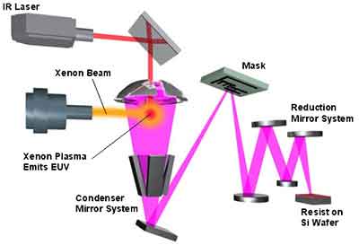
Modern high-volume EUV scanners use a laser-produced plasma (LPP) source. Small droplets of molten tin are introduced into the source chamber and irradiated by powerful laser pulses.
The laser interaction creates a hot tin plasma that emits radiation near the required 13.5 nm wavelength. A collector mirror captures part of this radiation and directs it into the illumination system.
Generating sufficiently powerful, stable EUV radiation is one of the major engineering challenges of EUV lithography because only a fraction of the generated radiation ultimately reaches the photoresist-coated wafer.
Why EUV Lithography Uses Mirrors Instead of Lenses
EUV radiation is strongly absorbed by most materials, including materials that can be used as transmissive optics at visible or DUV wavelengths. Consequently, conventional refractive lenses cannot be used to guide and focus 13.5 nm EUV radiation.
EUV scanners instead use highly engineered multilayer reflective optics. The mask used for EUV lithography is also reflective rather than transmissive.
Because EUV radiation is strongly absorbed by gases, the EUV optical path operates under vacuum conditions. This combination of reflective masks, multilayer mirrors, vacuum operation, and precise contamination control makes EUV considerably more complex than conventional optical lithography.
What Happens to the Wafer During EUV Lithography?
A semiconductor wafer undergoing EUV patterning is prepared with a photosensitive resist and positioned on a precision wafer stage. The patterned EUV radiation exposes selected regions of the resist according to the circuit design encoded by the reflective mask.
A simplified EUV patterning sequence can include:
- Prepare and clean the semiconductor wafer.
- Apply an EUV-sensitive photoresist.
- Align the wafer and reflective EUV mask.
- Expose the resist with patterned 13.5 nm EUV radiation.
- Develop the resist to reveal the patterned image.
- Transfer the pattern into or onto the underlying material.
- Remove or further process the remaining resist as required.
These lithography steps are repeated throughout semiconductor fabrication as different device and interconnect layers are constructed.
Silicon Wafers for EUV Lithography Research
EUV lithography is a patterning process rather than a specific wafer material. The appropriate substrate therefore depends on the device and experiment being fabricated.
Silicon wafers are widely used as starting substrates for semiconductor process research. Depending on the project, researchers may require specific diameter, orientation, resistivity, dopant, thickness, surface finish, TTV, bow, warp, or particle specifications.
Advanced device research may also use epitaxial silicon wafers, where a controlled crystalline layer is grown on a silicon substrate, or silicon-on-insulator (SOI) wafers, depending on the device architecture and process flow.
Why Wafer Quality Matters in Advanced Lithography
Lithographic performance is influenced not only by the exposure system but also by the wafer and the complete film stack being patterned. Advanced processes require precise control of wafer geometry and surface condition because lithography must maintain focus and overlay across the patterned area.
Depending on the experiment, important wafer specifications can include:
- Total Thickness Variation (TTV)
- Bow and warp
- Surface roughness
- Particle and contamination levels
- Crystal orientation
- Resistivity and dopant type
- Polished surface quality
- Epitaxial layer specifications, when applicable
- SOI device and buried oxide thickness, when applicable
The exact substrate requirements are determined by the semiconductor process flow rather than by EUV exposure alone.
EUV Photoresist and Stochastic Effects
Photoresist performance is particularly important in EUV lithography. Because EUV exposure involves a finite number of high-energy photons, statistical variations in photon absorption and subsequent chemical reactions can contribute to stochastic variation.
At very small dimensions, these effects can contribute to line-edge roughness, linewidth variation, incomplete features, bridging, or other pattern defects. Researchers therefore work to balance resolution, sensitivity, roughness, and defectivity when developing EUV resist systems.
EUV Masks and Pattern Transfer
EUV masks differ fundamentally from conventional transmissive photomasks. Because 13.5 nm radiation cannot efficiently pass through conventional mask substrates, an EUV mask uses a reflective multilayer structure.
Patterned absorber structures on the mask modify the reflected EUV radiation to create the image that is projected onto the wafer. Mask defects, contamination, three-dimensional mask effects, and imaging performance are therefore important considerations in advanced EUV process development.
Does Intel Use EUV Lithography?
Yes. Intel introduced EUV into high-volume manufacturing with its Intel 4 process technology. EUV is used extensively in that process to enable advanced patterning and simplify portions of the manufacturing flow that could otherwise require more complex multiple-patterning approaches.
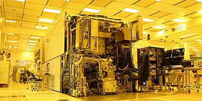
EUV is now an important technology for manufacturing leading-edge processors and other high-density integrated circuits. Its importance extends to chips used for artificial intelligence, high-performance computing, mobile electronics, data centers, and other demanding applications.
What Is High-NA EUV Lithography?
High-NA EUV is the next generation of EUV lithography. "NA" means numerical aperture, an optical parameter that influences imaging resolution.
Conventional production EUV systems use projection optics with an NA of approximately 0.33. High-NA EUV increases this to approximately 0.55 while continuing to use 13.5 nm EUV radiation.
The higher numerical aperture enables improved resolution, but High-NA also introduces new engineering and process-integration challenges involving optics, masks, resist processes, depth of focus, metrology, overlay, and pattern transfer.
EUV Lithography vs. DUV Lithography
EUV does not completely replace DUV photolithography. Semiconductor fabs use different lithography technologies according to the resolution, cost, process, and layer requirements.
ArF DUV lithography operates at 193 nm, while EUV uses approximately 13.5 nm. EUV's much shorter wavelength enables finer patterning and can reduce the number of multiple-patterning steps required for some critical layers.
DUV remains important for many semiconductor layers where its resolution and economics are appropriate. Modern chip fabrication therefore uses a combination of lithography and patterning technologies rather than EUV for every layer.
What Is EUV Lithography Used to Manufacture?
EUV is primarily associated with critical patterning layers in leading-edge semiconductor manufacturing. Devices manufactured using process flows that incorporate EUV can include:
- Advanced CPUs and microprocessors
- AI accelerators
- Graphics processors (GPUs)
- Data-center processors
- Advanced mobile processors
- High-density memory devices
- High-performance system-on-chip (SoC) devices
- Other leading-edge integrated circuits
EUV is one component of the complete manufacturing process. Device performance also depends on transistor architecture, materials, deposition, etching, implantation, interconnect technology, packaging, and many other fabrication steps.
Semiconductor Substrates for Lithography Research
UniversityWafer supplies semiconductor substrates for lithography, thin-film processing, etching, deposition, device fabrication, and semiconductor process-development research.
When requesting wafers for advanced lithography research, specify the substrate material, diameter, thickness, orientation, resistivity, dopant, surface finish, TTV, bow, warp, film stack, and quantity whenever those parameters are known.
Get Your Semiconductor Wafer Quote FAST!
Or,
Buy Wafers Online
and Start Researching Today!
What Is Extreme Ultraviolet Lithography (EUV)?
Extreme ultraviolet lithography (EUV) is a projection lithography technology used to pattern critical layers in advanced semiconductor manufacturing. EUV scanners operate near a wavelength of 13.5 nanometers (nm), compared with 193 nm for ArF deep ultraviolet (DUV) lithography.
EUV exposes a photosensitive resist according to a circuit pattern. After the resist is developed, the resulting pattern can be transferred into an underlying material through processes such as etching or used during deposition, implantation, and other semiconductor fabrication steps.
EUV's much shorter wavelength enables higher-resolution patterning and can reduce the number of multiple-patterning steps required for some critical layers compared with 193 nm DUV processes.
How Does EUV Lithography Work?
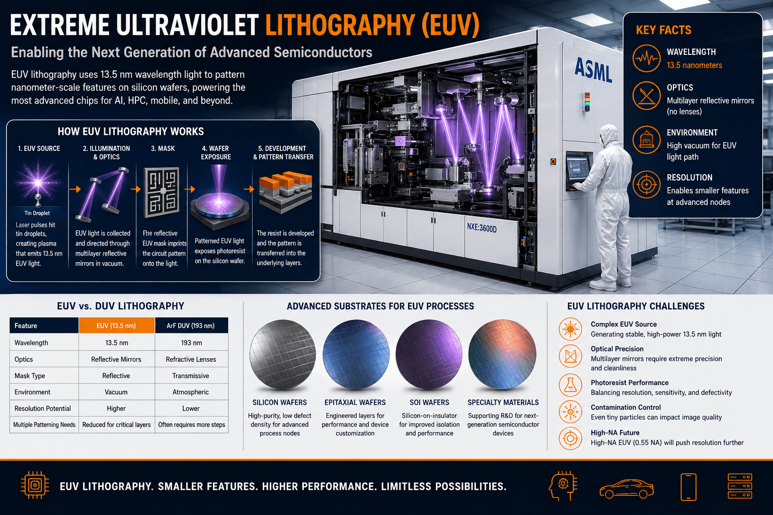
Production EUV systems use a laser-produced plasma (LPP) source. Small droplets of tin are irradiated by high-power laser pulses, creating a plasma that emits radiation near 13.5 nm.
A collector directs EUV radiation into an optical system composed of specialized multilayer mirrors. The illumination reaches a reflective EUV mask, and projection optics form a reduced image of the mask pattern on a photoresist-coated wafer.
Because EUV radiation is strongly absorbed by gases and most materials, the EUV optical path operates under vacuum and uses reflective optics instead of conventional transmissive lenses.
Why Does EUV Use Reflective Multilayer Mirrors?
Materials that are transparent enough to function as conventional refractive lenses at visible or DUV wavelengths strongly absorb 13.5 nm EUV radiation. EUV scanners therefore rely on multilayer reflective optics.
EUV mirrors commonly use carefully engineered alternating multilayers designed to provide constructive reflection near the operating wavelength. Even these mirrors reflect only part of the incident EUV radiation, so losses accumulate as the light travels through the optical system.
Mirror surface figure, roughness, multilayer quality, contamination, and thermal stability must therefore be tightly controlled to maintain imaging performance and EUV throughput.
What Is an EUV Mask?
Unlike many DUV photomasks, an EUV mask is reflective. It contains a multilayer reflector and patterned absorber structures that modify the reflected EUV radiation according to the desired circuit layout.
EUV mask performance is important because defects, contamination, absorber geometry, multilayer variations, and three-dimensional mask effects can influence the image projected onto the wafer.
Mask inspection, defect control, cleaning, repair, and computational correction are therefore important parts of EUV process development.
What Is an EUV Pellicle?
A pellicle is a very thin membrane positioned above the patterned surface of a photomask to help prevent particles from landing directly on the mask pattern.
EUV pellicles present a particularly difficult engineering problem because the membrane must transmit a large fraction of the EUV radiation while remaining mechanically stable and tolerating significant thermal loading.
Pellicle transmission and durability affect scanner throughput and mask protection, making pellicle materials and thermal management important areas of EUV technology development.
EUV Photoresist and Pattern Formation
Before EUV exposure, the wafer is coated with an EUV-sensitive photoresist. Absorption of EUV photons initiates chemical changes that allow exposed and unexposed regions to respond differently during resist development.
EUV resist design requires balancing several competing requirements, including:
- High imaging resolution
- Adequate EUV sensitivity
- Low line-edge and linewidth roughness
- Low stochastic defectivity
- Sufficient etch resistance
- Film uniformity
- Compatibility with subsequent pattern-transfer processes
Improving one resist characteristic can affect another, which makes photoresist optimization one of the central challenges of EUV lithography.
What Are Stochastic Defects in EUV Lithography?
At extremely small dimensions, the discrete nature of photon absorption and resist chemistry becomes increasingly important. Statistical variations in the number and spatial distribution of absorbed photons, together with variations in chemical reactions within the resist, can produce stochastic patterning effects.
Depending on the pattern and process, stochastic variation can contribute to defects such as:
- Line-edge roughness
- Line-width roughness
- Missing or incompletely formed features
- Bridging between nearby features
- Local critical-dimension variation
EUV process development therefore requires optimization of exposure dose, resist chemistry, feature geometry, development conditions, and subsequent pattern transfer.
What Determines EUV Lithography Resolution?
Lithographic resolution is influenced by the exposure wavelength, numerical aperture, illumination, mask design, resist behavior, process conditions, and computational imaging techniques.
A commonly used simplified relationship is:
Resolution ≈ k1 × λ / NA
where λ is wavelength, NA is numerical aperture, and k1 represents process and imaging factors.
This relationship helps explain why the combination of a 13.5 nm wavelength and advanced projection optics enables EUV to pattern finer features than conventional 193 nm optical lithography under comparable imaging conditions.
What Is High-NA EUV Lithography?
High-NA EUV increases the numerical aperture of the projection optics from approximately 0.33 in conventional EUV systems to 0.55, while continuing to operate near 13.5 nm.
Increasing NA improves achievable imaging resolution, but it also changes important aspects of the lithography system and process.
High-NA development must address challenges involving:
- Reduced depth of focus
- Mask imaging and three-dimensional mask effects
- Photoresist performance
- Overlay and focus control
- Metrology and defect inspection
- Pattern transfer
- Scanner throughput and process integration
EUV vs. DUV Lithography
EUV and DUV lithography are both important semiconductor patterning technologies, but they operate at very different wavelengths.
| Property | EUV Lithography | ArF DUV Lithography |
|---|---|---|
| Nominal Wavelength | 13.5 nm | 193 nm |
| Projection Optics | Reflective multilayer mirrors | Primarily refractive optical systems |
| Mask | Reflective | Transmissive |
| Optical Environment | Vacuum | Does not require an EUV-style vacuum optical path |
| Patterning Role | Critical advanced layers requiring very high resolution | Used extensively across many semiconductor layers |
| Multiple Patterning | Can reduce multiple-patterning requirements for some critical layers | Multiple patterning can extend 193 nm lithography to smaller pitches |
EUV does not eliminate DUV lithography. Modern semiconductor manufacturing uses the lithography technology appropriate for each layer according to resolution, process integration, throughput, and cost requirements.
Overlay and Critical Dimension Control in EUV
Semiconductor devices contain many patterned layers that must be aligned with high precision. Overlay describes the alignment accuracy between one patterned layer and another.
Critical dimension (CD) describes the size of an important patterned feature, such as a line width or space. Variation in CD can influence electrical and manufacturing performance.
EUV manufacturing therefore depends on precise wafer positioning, alignment, focus control, mask characterization, process control, and semiconductor metrology.
Why Wafer Flatness and Surface Quality Matter
EUV exposure is only one part of a complex semiconductor fabrication process. The wafer and film stack must also satisfy demanding geometry, surface, contamination, and process-integration requirements.
Depending on the application, important substrate parameters can include:
- Total Thickness Variation (TTV)
- Bow and warp
- Surface roughness
- Particle contamination
- Crystal orientation
- Resistivity and doping
- Film thickness and uniformity
- Epitaxial layer properties
- SOI device-layer and buried-oxide thickness
These parameters do not determine EUV resolution by themselves, but wafer geometry and process-stack control are important for focus, overlay, pattern transfer, device fabrication, and overall process yield.
Silicon, Epitaxial and SOI Wafers for Advanced Lithography
Silicon wafers remain a fundamental substrate platform for semiconductor process development and integrated-circuit fabrication.
Depending on the device architecture, advanced research can also use epitaxial silicon wafers with controlled crystalline device layers or silicon-on-insulator (SOI) wafers containing a silicon device layer separated from the handle substrate by a buried insulating layer.
The choice between bulk silicon, epitaxial silicon, SOI, and other semiconductor substrates is determined by the device architecture and process flow—not by the use of EUV lithography alone.
Pattern Transfer After EUV Exposure
Creating the resist image is not the final fabrication step. After lithography, the resist pattern must often be transferred into an underlying film using processes such as plasma etching.
Advanced semiconductor structures also require repeated cycles of lithography together with deposition, etching, cleaning, implantation, annealing, planarization, and metrology.
Processes such as atomic layer deposition (ALD), chemical vapor deposition (CVD), and chemical mechanical polishing (CMP) can therefore be closely related to the overall fabrication flow in which EUV patterning is used.
Applications of EUV Lithography
EUV is used for selected critical layers in advanced semiconductor manufacturing. Process technologies incorporating EUV can be used to manufacture devices such as:
- Advanced CPUs
- AI accelerators
- Graphics processors (GPUs)
- High-performance computing processors
- Mobile system-on-chip (SoC) devices
- Advanced memory devices
- Data-center processors
- Other high-density integrated circuits
EUV enables finer patterning and can simplify certain patterning sequences, but improvements in device speed, power efficiency, and transistor density result from the complete device architecture and manufacturing process, not from EUV exposure alone.
Major Challenges in EUV Semiconductor Manufacturing
EUV lithography combines demanding optical, plasma, materials, mechanical, vacuum, chemical, and computational engineering requirements.
Important challenges include:
- Generating sufficient stable EUV source power
- Managing optical losses through the reflective system
- Controlling contamination of EUV optics
- Detecting and controlling mask defects
- Developing durable, high-transmission pellicles
- Balancing resist resolution, sensitivity and roughness
- Reducing stochastic patterning defects
- Maintaining precise focus and overlay
- Controlling critical dimensions
- Achieving reliable pattern transfer
- Maintaining manufacturing throughput and yield
The Future of EUV and High-NA EUV
EUV is an established patterning technology in leading-edge semiconductor manufacturing, while High-NA EUV is being developed and introduced to extend EUV imaging capability further.
Continued progress depends not only on scanner optics but also on improvements in photoresists, masks, pellicles, computational lithography, metrology, pattern transfer, materials, wafer processing, and overall process integration.
As semiconductor structures become increasingly complex, EUV and High-NA EUV are expected to remain important tools for patterning selected critical layers where their resolution capabilities provide manufacturing benefits.