
What Silicon-on-Insulator (SOI) Wafer Specifications Do I Need?
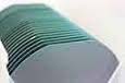 Selecting the correct Silicon-on-Insulator (SOI) wafer begins with understanding your device requirements. Researchers developing CMOS integrated circuits, MEMS devices, RF components, silicon photonics, power electronics, and advanced sensors typically specify the thickness of the silicon device layer, the buried oxide (BOX) layer, handle wafer thickness, crystal orientation, dopant type, resistivity, polish, and wafer diameter.
Unlike conventional bulk silicon wafers, SOI wafers electrically isolate the active silicon layer from the substrate using a precisely controlled silicon dioxide layer. This unique structure reduces parasitic capacitance, minimizes leakage current, improves switching speed, and enables smaller, more energy-efficient semiconductor devices.
UniversityWafer supplies both Bonded SOI wafers and SIMOX SOI wafers with custom device-layer thicknesses, buried oxide thicknesses, and handle wafer specifications. Whether your application involves microelectronics, MEMS fabrication, silicon photonics, RF devices, or aerospace electronics, we can help identify the ideal SOI substrate for your process.
Typical SOI Wafer Specifications
- Wafer Diameter: 2", 3", 4", 6", 8", and 12"
- Device Layer Thickness: From a few nanometers to hundreds of microns
- Buried Oxide (BOX) Thickness: Typically 100 nm to several microns
- Handle Wafer Thickness: Standard or custom thicknesses
- Crystal Orientation: <100>, <111>, and other orientations
- Dopant Type: Boron (P-type), Phosphorus, Arsenic, or Antimony (N-type)
- Resistivity: Low, medium, or high resistivity depending on the application
- Surface Finish: Single-Side Polished (SSP) or Double-Side Polished (DSP)
Get Your SOI Wafer Quote FAST! Or, Buy Online and Start Researching Today!
Typical applications include:
- CMOS integrated circuits
- MEMS fabrication
- Silicon photonics
- RF integrated circuits
- Microfluidic devices
- Optical sensors
- Power semiconductor research
The excellent control of both the silicon device layer and buried oxide thickness allows engineers to optimize electrical isolation, mechanical properties, and optical performance for demanding applications.
SIMOX (Separation by Implanted Oxygen)
SIMOX SOI wafers are manufactured by implanting high-energy oxygen ions into a silicon wafer followed by high-temperature annealing. During annealing, the implanted oxygen reacts with silicon to form a continuous buried silicon dioxide (BOX) layer beneath the wafer surface.
The implantation energy determines the depth of the buried oxide, while the implantation dose controls oxide formation. This process creates an SOI structure without bonding two separate wafers.
SIMOX technology is frequently selected for:
- Radiation-hardened electronics
- Military electronics
- Spacecraft and satellite systems
- Low-power integrated circuits
- High-reliability semiconductor devices
Because the buried oxide is formed directly inside the silicon crystal, SIMOX wafers provide excellent electrical isolation and long-term reliability for specialized applications.
Smart Cut® SOI Technology
Smart Cut® technology combines wafer bonding with hydrogen ion implantation to produce extremely uniform device layers. Hydrogen ions are implanted at a precisely controlled depth within the donor wafer before bonding it to an oxidized handle wafer.
Following thermal treatment, the implanted hydrogen forms microscopic cavities that allow the upper silicon layer to separate cleanly from the donor wafer. The transferred silicon layer becomes the active device layer of the finished SOI wafer, while the remaining donor wafer can often be reclaimed and reused for future production.
Smart Cut® technology provides several important advantages:
- Excellent device-layer thickness uniformity
- Low defect density
- High wafer yield
- Reduced manufacturing cost through donor wafer reuse
- Compatibility with advanced CMOS manufacturing
Today, many commercial SOI wafers used in semiconductor manufacturing, MEMS fabrication, and silicon photonics are produced using Smart Cut® technology because of its precision and scalability.
Choosing the Right SOI Manufacturing Method
The most appropriate SOI wafer depends on the intended application, fabrication process, and device requirements. Engineers typically compare manufacturing methods based on electrical performance, mechanical stability, oxide quality, and manufacturing cost.
| Manufacturing Method | Main Advantages | Typical Applications |
|---|---|---|
| Bonded SOI | Excellent thickness uniformity, low defect density, customizable device layers | CMOS, MEMS, RF, silicon photonics, sensors |
| SIMOX | Outstanding electrical isolation and radiation tolerance | Defense, aerospace, radiation-hardened electronics |
| Smart Cut® | Ultra-uniform device layer, high production yield, reusable donor wafers | Advanced CMOS, high-volume manufacturing, photonics |
How to Select the Right SOI Wafer
Selecting the appropriate SOI wafer depends on your fabrication process, device architecture, and performance requirements. Engineers should consider several key specifications before ordering:
- Device Layer Thickness – Determines the active silicon available for transistors, MEMS structures, or photonic waveguides.
- Buried Oxide (BOX) Thickness – Controls electrical isolation, optical confinement, and etch-stop performance.
- Handle Wafer Thickness – Provides mechanical support during wafer processing.
- Crystal Orientation – Commonly <100> or <111> depending on the fabrication process.
- Dopant Type and Resistivity – Selected according to CMOS, RF, MEMS, or sensor requirements.
- Surface Finish – SSP or DSP depending on lithography and bonding requirements.
How Is an SOI Wafer Constructed?
A Silicon-on-Insulator (SOI) wafer consists of three primary layers that work together to improve electrical performance and simplify semiconductor fabrication.
- Device Layer: The thin silicon layer where transistors, MEMS structures, photonic waveguides, or other active devices are fabricated.
- Buried Oxide (BOX) Layer: A layer of silicon dioxide (SiO₂) that electrically isolates the device layer from the handle wafer. The BOX layer reduces parasitic capacitance, lowers leakage current, and improves device isolation.
- Handle Wafer: A thicker silicon substrate that provides mechanical strength during wafer processing and device fabrication.
How Are SOI Wafers Manufactured?
Several manufacturing techniques are used to produce Silicon-on-Insulator (SOI) wafers. Although each method creates the same basic three-layer structure, the manufacturing process influences wafer quality, device-layer uniformity, buried oxide characteristics, and the types of applications for which the wafer is best suited.
The three most common SOI manufacturing methods are wafer bonding, SIMOX (Separation by IMplanted OXygen), and Smart Cut® technology. Each process offers unique advantages for semiconductor manufacturing, MEMS fabrication, RF devices, and silicon photonics.
Bonded SOI Wafers
Bonded SOI wafers are produced by joining two polished silicon wafers together with a carefully grown silicon dioxide layer between them. After bonding, one wafer is thinned by grinding, chemical mechanical polishing (CMP), or Smart Cut® processing until the desired device-layer thickness is achieved.
This manufacturing method produces excellent thickness uniformity, low defect density, and a high-quality silicon-to-oxide interface. Because of these characteristics, bonded SOI wafers have become the preferred choice for many advanced semiconductor applications.
Common SOI Wafer Applications
Silicon-on-Insulator (SOI) wafers are used when engineers need better electrical isolation, lower leakage current, reduced parasitic capacitance, and improved device performance compared with standard bulk silicon wafers. An SOI wafer includes a thin active silicon device layer, a buried oxide layer (BOX), and a silicon handle substrate. This structure makes SOI useful for CMOS, MEMS, silicon photonics, RF devices, sensors, and radiation-hardened electronics.
UniversityWafer supplies bonded SOI wafers, SIMOX SOI wafers, custom device-layer thicknesses, buried oxide thicknesses, and handle wafer specifications for research, prototyping, and production applications.
SOI Wafers for CMOS and Low-Power Electronics
SOI wafers are widely used in CMOS and low-power integrated circuits because the buried oxide layer helps reduce unwanted electrical interaction between the active silicon device layer and the handle substrate. This can improve switching speed, reduce leakage current, and lower power consumption.
For mobile electronics, IoT devices, and high-speed logic, these advantages are important because chip designers must balance speed, heat generation, and battery life. Bonded SOI wafers are commonly selected when tight device-layer uniformity and high-quality interfaces are required.
SOI Wafers for RF and Wireless Devices
Radio-frequency devices often require excellent electrical isolation and low substrate loss. SOI wafers can help improve RF performance by reducing parasitic capacitance and limiting signal coupling through the substrate. For this reason, SOI is used in RF switches, tuners, filters, front-end modules, and wireless communication components.
High-resistivity SOI wafers are especially useful for RF applications because they help reduce signal loss and improve device efficiency. Researchers and manufacturers may specify device-layer thickness, BOX thickness, handle resistivity, orientation, and wafer diameter depending on the RF design.
SOI Wafers for MEMS Devices
MEMS devices benefit from SOI wafers because the device layer can act as a precisely controlled mechanical structure. The buried oxide layer is often used as an etch-stop layer during micromachining, allowing repeatable fabrication of membranes, beams, cavities, sensors, and actuators.
Common MEMS applications include pressure sensors, accelerometers, gyroscopes, micro-mirrors, resonators, microphones, and biomedical sensors. Bonded SOI wafers are frequently selected for MEMS because they offer excellent control over device-layer thickness and mechanical uniformity.
SOI Wafers for Silicon Photonics
SOI wafers are one of the most important substrates for silicon photonics. The top silicon layer can be patterned into waveguides, while the buried oxide layer provides optical confinement. This makes SOI useful for photonic integrated circuits, optical modulators, grating couplers, interferometers, and on-chip optical sensors.
Photonics-grade SOI wafers often require carefully controlled device-layer thickness, low surface roughness, and a high-quality buried oxide layer. These properties help reduce optical loss and improve device performance in communications, LiDAR, biosensing, and integrated optics research.
SOI Wafers for Radiation-Hardened Electronics
SOI wafers are also used in aerospace, satellite, military, and high-reliability electronics because the buried oxide layer helps isolate devices from the bulk substrate. This isolation can reduce radiation-induced leakage paths and improve resistance to certain radiation effects.
SIMOX SOI wafers are often associated with radiation-hardened applications because the buried oxide layer is formed by oxygen implantation and high-temperature annealing. Depending on the device design, both SIMOX and bonded SOI wafers may be used for radiation-tolerant circuits.
Bonded SOI vs. SIMOX SOI
The two most common SOI wafer types are bonded SOI and SIMOX SOI. Each has advantages depending on the application.
| SOI Type | How It Is Made | Common Uses |
|---|---|---|
| Bonded SOI | Two silicon wafers are bonded with an oxide layer between them, then thinned and polished to the target device-layer thickness. | MEMS, CMOS, silicon photonics, sensors, custom research wafers. |
| SIMOX SOI | Oxygen ions are implanted into silicon and annealed to form a buried oxide layer below the surface. | Radiation-hardened electronics, low-power devices, specialty semiconductor research. |
Important SOI Wafer Specifications
When selecting an SOI wafer, the most important specifications are the device-layer thickness, buried oxide thickness, handle wafer thickness, crystal orientation, dopant type, resistivity, polish, and wafer diameter. These parameters directly affect electrical behavior, mechanical performance, optical confinement, and process compatibility.
| Specification | Why It Matters |
|---|---|
| Device Layer Thickness | Controls the active silicon layer used for CMOS, MEMS structures, waveguides, and sensors. |
| Buried Oxide Thickness | Provides electrical isolation, optical confinement, and an etch-stop layer for MEMS fabrication. |
| Handle Wafer Thickness | Provides mechanical support during processing and handling. |
| Resistivity | Important for RF, power, sensor, and low-leakage applications. |
| Orientation | Affects etching behavior, mechanical response, and device design. |
| Polish | SSP or DSP may be required depending on bonding, lithography, MEMS, or optical processing needs. |
Why Choose SOI Wafers?
SOI wafers are chosen because they give engineers more control over the electrical, mechanical, and optical behavior of a device. Compared with bulk silicon, SOI can provide improved isolation, reduced leakage, better switching speed, and more repeatable device structures.
Whether the application is MEMS, RF, CMOS, photonics, aerospace electronics, or advanced sensors, SOI wafers allow researchers to design devices with a defined active silicon layer and a controlled buried oxide layer.