Custom Fabrication Case Studies: SiO2 for MEMS & Solar
UniversityWafer, Inc. delivers high-precision SiO2 deposition and Thermal Oxide services tailored for semiconductor research and volume production. We specialize in complex film stacks ranging from 50nm to 20µm, offering Wet/Dry Thermal Oxide, PECVD, and TEOS deposition on Silicon, Fused Silica, and SOI substrates. Whether for MEMS, Solar, or optical applications, our custom fabrication ensures superior uniformity and low metal contamination.
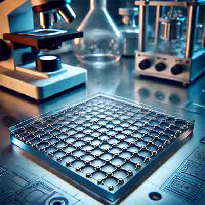
A university student researcher requested a quote for the following ![]() SiO2 coated wafers:
SiO2 coated wafers:
Case Study 1: Multi-Layer Stack for MEMS Energy Harvesting
Client: University Researcher (MEMS)
Application: Piezoelectric Energy Harvesting Device
A researcher required a custom 5-layer stack on a 2-inch silicon substrate to fabricate a piezo-based harvester. We delivered the following specification:
- Substrate: 2" Silicon Wafer (P-type or N-type)
- Layer 1: 500nm Thermal Oxide (SiO2)
- Layer 2: 500nm Titanium (Adhesion/Bottom Electrode)
- Layer 3: 2µm PZT or ZnO (Piezoelectric Material)
- Layer 4: 500nm Titanium (Top Electrode)
Solution: We utilized our precise deposition capabilities to ensure adhesion between the Titanium and SiO2 layers.
(Reference #120417)
Case Study 2: 300mm Wafers for Solar Manufacturing
Client: Principal Engineer (Solar Panel Manufacturer)
A major solar manufacturer required large-diameter substrates for process calibration. While dopant and orientation were flexible, surface purity was non-negotiable.
- Substrate: 300mm (12 inch) Silicon Wafers
- Configuration: Bare Si or SiO2 Coated
- Critical Requirement: Ultra-low metal contamination
Solution: We supplied wafers meeting strict contamination protocols suitable for photovoltaic research.
(Reference #94346)
Get Your Quote FAST! Or, Buy Online and Start Researching Today!
SiO2 Deposition Services: Thermal Oxide, PECVD & TEOS
| Coating Types | Thermal Oxide (Wet/Dry), PECVD, TEOS, Native Oxide |
|---|---|
| Thickness Range | 50nm to 20µm (Customizable) |
| Substrate Diameters | 25mm, 50mm, 76mm, 100mm, 150mm, 200mm, 300mm |
| Base Materials | Silicon (Si), Fused Silica, SOI, Borofloat 33, Quartz |
| Key Applications | Gate Oxides, MEMS, Passivation, Electrical Insulation, Optical Coatings |
Properties of High-Purity SiO2 Coatings
Silicon dioxide (SiO2) is a chemical compound composed of one silicon atom and two oxygen atoms. Nature's abundant with this stuff, showing up as quartz and even inside living things. With silica making up a significant chunk of sand, it's no wonder industries have grown to rely on its specialized set of physical and chemical characteristics.
Key properties and uses of SiO2 include:
-
Glass Production: SiO2 is the primary ingredient in glass manufacturing. Glassmaking begins with molten heat, slowly cooled to form a transparent solid. This cooled glass then finds its way into everyday items like windows, bottles, and more.
-
Electronics: High-purity SiO2 is used to manufacture semiconductors and insulators in electronic devices. Silicon chip and integrated circuit production rely heavily on this vital component.
-
Construction: SiO2 is used as a key ingredient in cement and concrete, providing strength and durability to construction materials.
-
Abrasives: Due to its hardness, SiO2 is used in sandblasting and as a filler in abrasive materials like sandpaper.
-
Optics: SiO2 is used in the production of optical fibers and lenses due to its transparency and ability to withstand high temperatures.
-
Health and Food Industry: SiO2 is used as an anti-caking agent in powdered foods and in pharmaceuticals to ensure consistency and flowability of products.
-
Natural Occurrence: SiO2 occurs naturally in various forms, including quartz, cristobalite, tridymite, and lechatelierite, each with unique physical properties.
SiO2 stands out from the pack thanks to its triple threat of advantages. It's impervious to chemical reactions, brutally resistant to wear and tear, and has a melting point that's basically sci-fi. Little wonder it's the material of choice for numerous industries.
Semiconductor Applications: Gate Oxide, Passivation & Insulation
Silicon dioxide (SiO2) plays a crucial role in the semiconductor industry. Its unique properties make it indispensable in the manufacturing and functioning of semiconductor devices. Here are some key ways SiO2 is used in semiconductors:
-
Insulating Layer: SiO2 is used as an insulator between different layers of silicon in semiconductor
 devices. Its excellent insulating properties prevent electrical current from leaking between layers, which is critical for the proper functioning of electronic components.
 -
Gate Oxide in MOSFETs: In Metal-Oxide-Semiconductor Field-Effect Transistors (MOSFETs), SiO2 is used to form the gate oxide layer. This thin layer of SiO2 separates the metal gate from the silicon substrate, controlling the flow of current through the transistor. The quality and thickness of this oxide layer are crucial for the performance and reliability of MOSFETs.
-
Dielectric Material: SiO2 acts as a dielectric material in capacitors within integrated circuits (ICs). It stores electric charge and helps in maintaining the stability and performance of the ICs.
-
Passivation Layer: SiO2 is used as a passivation layer to protect the surface of semiconductor devices from contamination and environmental damage. This layer helps in improving the reliability and longevity of the devices.
-
Interlayer Dielectric: In multi-layer semiconductor devices, SiO2 is used as an interlayer dielectric to electrically isolate different conducting layers. This allows for the creation of complex, multi-layered integrated circuits.
-
Doping Process: During the doping process, SiO2 layers can be used to mask certain areas of the silicon wafer, allowing selective doping of the silicon substrate. This process is essential for creating p-n junctions and other semiconductor structures.
-
Etching and Patterning: SiO2 layers are used in photolithography and etching processes to define and pattern specific areas of the silicon wafer. This is a key step in the fabrication of semiconductor devices, enabling the creation of intricate and precise circuit patterns.
The use of SiO2 in semiconductors is fundamental to the performance, efficiency, and miniaturization of modern electronic devices. Its ability to act as an insulator, dielectric, and protective layer makes it a versatile and essential material in the semiconductor industry.
