Amorphous Silicon Thin Films on Transparent Substrates
Amorphous silicon (a-Si), particularly hydrogenated amorphous silicon (a-Si:H), can be deposited as a thin film on compatible substrates for optical, electronic, photovoltaic, lithographic, and materials-science research. Transparent substrates such as
fused silica
and selected glass materials are especially useful when optical transmission through the substrate is required.
A master's-level researcher requested:
For one of our experiments we are looking for
thin films
of amorphous
silicon
on a transparent
substrate.
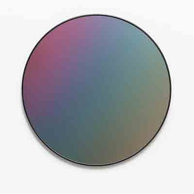
I am looking for a 4-inch double-side-polished fused silica or quartz substrate with an amorphous silicon layer.
I was wondering if UniversityWafer can provide amorphous Si on quartz wafers or a similar transparent substrate.
Reference #90835 for historical specifications and pricing.
When requesting amorphous silicon coatings, specify the substrate material, dimensions, a-Si film thickness, deposition side, allowable temperature, and any electrical, optical, stress, or surface requirements.
Get Your Amorphous Silicon Quote FAST!
Or,
Buy Wafers Online
and Start Researching Today!
Amorphous Silicon on Fused Silica
Fused silica
is an attractive substrate for amorphous-silicon thin films because of its optical transparency, electrical insulation, chemical stability, and low thermal expansion. The combination can be useful for optical experiments, patterned thin films, sensors, and nanostructure fabrication.
A researcher requested:
I am looking to buy one 4-inch double-side-polished fused silica/quartz wafer with an approximately 50 nm amorphous silicon layer. Film thickness, price, and lead time are the most important specifications.
Reference #267283 for historical specifications and pricing.
For thin a-Si coatings on fused silica, important parameters can include film thickness and uniformity, residual stress, adhesion, surface roughness, hydrogen content, optical constants, and the thermal budget of the substrate and subsequent fabrication steps.
How Are Amorphous Silicon Thin Films Deposited?
Several deposition techniques can be used to form amorphous silicon films. The appropriate process depends on the required film composition, hydrogen content, thickness, substrate material, temperature limit, and intended application.
Plasma-Enhanced Chemical Vapor Deposition (PECVD)
PECVD
is widely used to deposit hydrogenated amorphous silicon (a-Si:H). Plasma activation allows deposition at temperatures substantially below those required for many conventional thermal CVD processes. Hydrogen incorporated into the film can passivate dangling bonds in the disordered silicon network, reducing electrically active defect states.
Physical Vapor Deposition
Silicon films can also be produced using physical vapor deposition techniques such as sputtering. Whether the resulting film is fully amorphous depends on deposition conditions including substrate temperature, deposition energy, pressure, and subsequent thermal processing.
Thermal Processing
The thermal history of an amorphous silicon film is important. Heating can change hydrogen content, stress, defect density, and other properties. At sufficiently high temperatures and appropriate conditions, amorphous silicon can begin to crystallize into polycrystalline silicon. The allowable thermal budget should therefore be considered when selecting both the substrate and deposition process.
Amorphous Silicon for Thin-Film Solar Cells
Hydrogenated amorphous silicon has been widely used as a semiconductor absorber in
thin-film photovoltaic devices.
Its strong optical absorption allows the active semiconductor layers to be much thinner than conventional crystalline-silicon wafers.
A typical a-Si:H photovoltaic device can use a p-i-n or n-i-p structure. The relatively thick intrinsic layer provides much of the optical absorption, while doped layers help establish the internal electric field needed to collect photogenerated carriers.
Amorphous-silicon photovoltaics should not be confused with modern silicon heterojunction (HJT) solar cells. HJT devices generally use a crystalline-silicon wafer as the primary absorber together with very thin intrinsic and doped a-Si:H layers for surface passivation and carrier-selective contacts. These are fundamentally different device structures from conventional thin-film a-Si:H solar cells.
Light-Induced Degradation in a-Si:H
A well-known property of hydrogenated amorphous silicon is the Staebler–Wronski effect. Prolonged illumination can produce metastable changes in the material that increase defect density and reduce photoconductivity and photovoltaic performance.
The effect is not accurately described as a fixed percentage loss or as degradation that always stops after a specific number of years. Its magnitude depends on material quality, device structure, illumination, operating temperature, and processing history.
Thermal annealing can reverse a substantial portion of these light-induced changes. In operating photovoltaic devices, light-induced defect creation and thermally activated recovery can both influence stabilized performance.
Amorphous Silicon vs. Amorphous Silica
Amorphous silicon and amorphous silica are different materials. This distinction is especially important when specifying substrates or coatings.
-
Amorphous silicon (a-Si): non-crystalline elemental silicon. Hydrogenated a-Si:H is commonly used as a semiconductor thin film.
-
Amorphous silica (SiO2): non-crystalline silicon dioxide, including high-purity fused silica. It is an electrically insulating oxide rather than a semiconductor equivalent of a-Si.
-
Crystalline silicon (c-Si): silicon with long-range crystal order, commonly supplied as single-crystal semiconductor wafers.
-
Polycrystalline silicon (poly-Si): silicon composed of multiple crystalline grains separated by grain boundaries.
Can Single-Crystal Silicon Be Deposited Directly on Glass?
Conventional deposition of silicon directly onto amorphous glass does not normally produce a single-crystal silicon layer. Single-crystal epitaxial growth generally requires an appropriate crystalline template so that the deposited material can maintain crystallographic registry with the underlying surface.
Silicon deposited directly onto glass is therefore typically amorphous or polycrystalline, depending on the deposition conditions and subsequent processing.
However, this does not mean that a structure containing single-crystalline silicon on glass is impossible. Specialized approaches such as wafer bonding, layer transfer, thinning, or related integration techniques can place a crystalline silicon layer onto a glass substrate without directly growing the single crystal on the amorphous glass surface.
For applications requiring a high-quality crystalline silicon film on an insulating crystalline substrate,
Silicon-on-Sapphire (SOS)
is another established material platform.
Silicon-on-Sapphire vs. Silicon-on-Glass
A researcher requested:
Do you have a silicon-on-glass substrate with approximately 1 µm of single-crystalline Si (100) over borosilicate glass or fused silica?
The answer depends strongly on how the silicon layer is produced. Direct thin-film deposition onto an amorphous glass substrate normally produces amorphous or polycrystalline silicon rather than epitaxial single-crystal Si. If single-crystalline silicon on glass is required, a transferred or bonded silicon layer may need to be considered.
Fused Silica for X-Ray Filter Research
Fused silica is itself an amorphous form of SiO2 and can be useful when an experiment requires a non-crystalline, electrically insulating material with well-controlled thickness and composition.
A corporate scientist requested:
I am looking to construct a filter for an X-ray application. It is important that the material be amorphous, pure, and have a well-characterized thickness.
I can model the filter using pure SiO2 approximately 100 µm thick, so I am interested in a
fused silica wafer
near this thickness.
Reference #195918 for historical specifications and pricing.
For X-ray transmission applications, material composition, density, thickness, thickness tolerance, surface condition, and the photon-energy range of interest should all be considered because X-ray attenuation is strongly energy dependent.
Amorphous Silicon on Quartz Wafers
Amorphous silicon deposited on quartz or fused-silica substrates can be useful for optical and nanofabrication research. The transparent substrate allows optical measurements through the sample while the deposited silicon layer can be patterned into nanoscale structures.
A researcher requested:
I was wondering if UniversityWafer provides amorphous silicon on
quartz wafers
or something similar. We are planning to use lithographic techniques to etch nanostructures and then investigate their optical properties.
For this type of application, researchers should consider a-Si film thickness, optical constants, surface roughness, film stress, etch selectivity, substrate transparency, and compatibility with the intended lithography and etching processes.
Reference #267283 for historical specifications and pricing.
Important Amorphous Silicon Research Terms
- Amorphous silicon (a-Si)
- Hydrogenated amorphous silicon (a-Si:H)
- Amorphous silicon thin films
- PECVD amorphous silicon
- Amorphous silicon on glass
- Amorphous silicon on fused silica
- Amorphous silicon on quartz
- Thin-film solar cells
- Thin-film transistors (TFTs)
- Photoconductivity
- Optical absorption
- Staebler–Wronski effect
- Film stress
- Surface roughness
- Silicon nanostructures
Amorphous Silicon for Materials Degradation Studies
Amorphous silicon (a-Si) thin films are useful for materials research where a non-crystalline silicon layer is required on glass, silicon, or other compatible substrates. Film thickness, substrate dimensions, deposition method, and surface requirements can be specified for the intended experiment.
A senior materials scientist requested the following:
We are looking for amorphous silicon of thickness approximately 0.5–1.0 µm deposited on a substrate. Our specifications are flexible; the substrate could be glass or another compatible material, ranging from approximately 10 × 10 mm pieces to 4-inch wafers.
Our application is fundamental studies of materials degradation in an EUV lithography environment. EUV lithography systems use Mo/Si multilayer reflective optics, and amorphous silicon films can be useful as model materials for studying silicon-containing layers under relevant experimental conditions.
UniversityWafer, Inc. Quoted:
100 mm diameter, 0.5 mm thick double-side-polished glass substrates with approximately 500 nm of amorphous silicon deposited on one side.
Reference #320377 for specifications and pricing.
What Is Amorphous Silicon?
Amorphous silicon (a-Si) is a non-crystalline form of silicon in which the atoms lack the long-range periodic arrangement found in single-crystal silicon. In electronic and optoelectronic applications, hydrogenated amorphous silicon (a-Si:H) is particularly important because hydrogen can passivate many dangling-bond defects in the disordered silicon network.
Unlike bulk crystalline silicon wafers, amorphous silicon can be deposited as a thin film over relatively large substrate areas. Depending on the required film properties and substrate temperature limits, deposition techniques can include chemical vapor deposition, PECVD, and physical vapor deposition methods such as sputtering.
The combination of thin-film processing, optical absorption, photosensitivity, and compatibility with large-area substrates has made a-Si:H important in photovoltaics, thin-film transistors, photodiodes, imaging arrays, and experimental thin-film structures.
Key Amorphous Silicon Applications
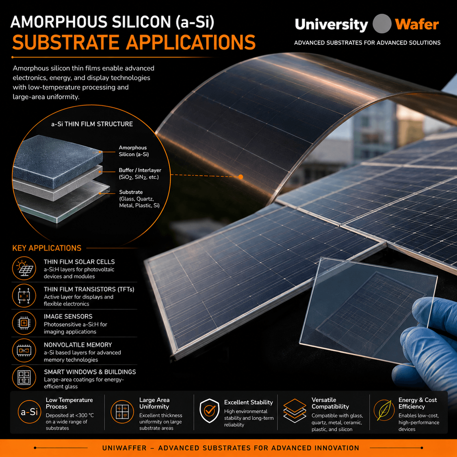
1. Thin-Film Solar Cells
Hydrogenated amorphous silicon has been widely studied and commercialized as an absorber material in thin-film photovoltaic cells. Because a-Si:H has strong optical absorption across much of the visible spectrum, photovoltaic absorber layers can be much thinner than conventional crystalline-silicon wafers.
Amorphous-silicon photovoltaic devices can be deposited on glass and other compatible substrates and have historically been used in calculators, small electronic devices, building-integrated photovoltaic products, and other thin-film solar applications.
A key limitation is light-induced metastability, commonly associated with the Staebler–Wronski effect. Prolonged illumination can increase defect density and reduce the stabilized photovoltaic performance of a-Si:H devices. Device architecture and material processing therefore play important roles in controlling long-term performance.
2. Amorphous Silicon Thin-Film Transistors
Hydrogenated amorphous silicon thin-film transistors (a-Si:H TFTs) have been extensively used as switching devices in active-matrix liquid-crystal displays (AMLCDs). Their major manufacturing advantages include good uniformity over large areas and compatibility with relatively low-temperature processing on glass substrates.
In a typical TFT, the a-Si:H layer forms the semiconductor channel whose conductivity is controlled by the gate voltage. Arrays containing millions of these transistors can independently address pixels across a large display panel.
A-Si:H has substantially lower carrier mobility than crystalline silicon and many modern oxide or polysilicon semiconductor technologies. However, its large-area uniformity and mature fabrication processes continue to make it useful where extremely high transistor mobility is not required.
3. Flat-Panel X-Ray Detectors
Amorphous silicon is also important in digital radiography and large-area X-ray imaging. In common indirect-conversion flat-panel detectors, incoming X-rays are first converted into visible light by a scintillator such as cesium iodide (CsI) or another suitable phosphor.
The resulting visible light is detected by an array of photodiodes, often based on a-Si:H, while thin-film transistors provide pixel addressing and electronic readout. Therefore, the amorphous silicon generally does not directly convert the incoming X-rays into electrical charge in this type of detector; it forms part of the photosensitive and readout structure.
This large-area thin-film architecture has been widely applied in medical radiography, fluoroscopy, nondestructive testing, and other digital X-ray imaging systems.
4. Photodiodes and Optical Sensors
The photosensitivity of a-Si:H also makes it useful for thin-film photodiodes and large-area optical sensor arrays. Light absorbed by the semiconductor generates electron-hole pairs that can contribute to a measurable photocurrent when the device is appropriately biased and structured.
Applications have included document scanners, contact image sensors, optical detection systems, and large-area imaging devices. Thin-film fabrication is particularly valuable when photosensitive elements must be distributed uniformly over an area much larger than a conventional discrete semiconductor chip.
5. Xerographic Photoreceptors
Amorphous silicon and related hydrogenated or alloyed amorphous-silicon materials have also been used as photoreceptor materials in electrophotographic systems. Their combination of photosensitivity, mechanical durability, and wear resistance can be advantageous for high-duty-cycle copier and printing applications.
Why Use Amorphous Silicon Thin Films?
The primary advantage of amorphous silicon is not simply that it is a less expensive version of crystalline silicon. Instead, a-Si offers a different set of processing and material characteristics that are particularly useful for large-area and thin-film devices.
- Thin-film deposition: Functional semiconductor layers can be deposited without growing and slicing a bulk single crystal.
- Large-area processing: a-Si:H can be deposited uniformly over relatively large glass and other compatible substrates.
- Relatively low processing temperatures: PECVD a-Si:H can be deposited at temperatures substantially below those required for growing bulk crystalline silicon.
- Strong optical absorption: Its disordered electronic structure gives a-Si:H strong absorption in much of the visible spectrum, which is useful for photodetectors and thin-film photovoltaics.
- Substrate flexibility: Depending on deposition temperature and process compatibility, amorphous silicon films can be formed on glass, silicon, metals, and selected temperature-resistant polymer substrates.
- Thickness control: Deposition processes allow researchers to specify films ranging from very thin layers to substantially thicker coatings for optical, electronic, or materials-science experiments.
Amorphous Silicon vs. Crystalline Silicon
| Property |
Amorphous Silicon |
Crystalline Silicon |
| Atomic Structure |
No long-range crystalline order |
Long-range periodic crystal lattice |
| Typical Form |
Deposited thin film |
Bulk wafer or epitaxial layer |
| Carrier Mobility |
Relatively low |
Much higher |
| Optical Absorption |
Strong across much of the visible spectrum |
Weaker near its indirect band edge |
| Large-Area Deposition |
Well suited |
Generally less suited to direct large-area thin-film deposition |
| Common Applications |
TFTs, photodiodes, X-ray detector arrays, thin-film PV |
Integrated circuits, MEMS, power devices, conventional PV |
Amorphous Silicon Deposited on Glass
Glass substrates are particularly useful for amorphous-silicon research because they provide an electrically insulating, optically useful, and relatively inexpensive platform for thin-film deposition. Substrate selection should account for deposition temperature, thermal expansion, surface roughness, chemical durability, and the requirements of subsequent processing.
Materials such as Borofloat 33 can be considered for research involving deposited silicon films, optical structures, sensors, and experimental devices when their thermal and chemical properties are compatible with the intended process.
Amorphous Silicon Deposited onto Borofloat 33
A research scientist requested:
Question:
Can you quote Borofloat 33 with approximately 1.5 µm of amorphous silicon deposited on each side?
We would like quantity 12 of 4-inch BF33 wafers, preferably with a major flat, with approximately 1.5 µm of amorphous silicon on both sides.
The deposited silicon is intended for use as a wet-etch mask.
Film deposition on both sides requires consideration of deposition method, achievable thickness, film stress, uniformity, substrate temperature limits, and whether the deposited silicon remains amorphous under the selected processing conditions.
Reference #91258 for historical specifications and pricing.
Amorphous Silicon for LCD Technology
In a conventional a-Si:H TFT-LCD, amorphous silicon is used primarily in the active-matrix transistor backplane rather than as the liquid-crystal material itself. Each TFT acts as an electronic switch that helps control the voltage applied to an individual pixel.
The ability to fabricate a-Si:H TFT arrays uniformly over large glass panels was one of the major reasons amorphous silicon became an important semiconductor technology for flat-panel displays.
Modern display technologies may also use alternatives such as low-temperature polysilicon (LTPS) or oxide semiconductors when higher carrier mobility or different electrical characteristics are required. Nevertheless, a-Si:H remains an important material in the history and engineering of large-area thin-film electronics.
Choosing an Amorphous Silicon Substrate
The appropriate substrate and film specification depend on the intended experiment or device. Important parameters can include:
- Substrate material and dimensions
- Amorphous silicon film thickness
- Single-side or double-side deposition
- Hydrogenated or non-hydrogenated film requirements
- Deposition method
- Film stress and adhesion
- Surface roughness
- Thickness uniformity
- Electrical resistivity or conductivity requirements
- Optical properties
- Maximum allowable substrate temperature
- Requirements for subsequent lithography, etching, or metallization
Clearly defining these parameters helps determine an appropriate combination of amorphous silicon film, substrate material, and deposition process for the intended research application.
Related Amorphous Silicon Resources
-
Silicon Wafers
– Explore silicon wafers and substrates for semiconductor, optical, and materials research.
-
Amorphous vs. Crystalline Silicon
– Learn how atomic structure affects the electrical, optical, and processing properties of silicon.
-
Thin Films
– Explore thin-film materials and deposited layers for research and device fabrication.
-
Chemical Vapor Deposition (CVD)
– Learn about CVD techniques used to deposit semiconductor and dielectric thin films.
-
Fused Silica Wafers
– Transparent amorphous SiO₂ substrates suitable for optical and thin-film research.
-
Quartz Wafers
– Explore crystalline quartz substrates for optical, electronic, and materials-science applications.
-
Borofloat 33 Glass
– Borosilicate glass substrates for deposited films, optical structures, and experimental devices.
-
Solar Cell Substrates
– Learn about semiconductor substrates and materials used in photovoltaic research.
-
Polycrystalline Silicon
– Compare polycrystalline silicon with amorphous and single-crystal silicon materials.
-
Silicon-on-Sapphire (SOS)
– Explore crystalline silicon layers on sapphire substrates for specialized electronic applications.
