
"We are designing MEMS pressure sensors using Silicon-on-Insulator wafers and require a 100 mm SOI substrate with a 20 μm device layer and a 2 μm buried oxide layer. Can you supply research quantities with custom specifications?"
Get Your SOI Wafer Quote FAST!
Developing a MEMS device, RF MEMS switch, pressure sensor, accelerometer, or silicon photonic circuit? UniversityWafer supplies high-quality Silicon-on-Insulator (SOI) wafers with custom device-layer thicknesses, buried oxide (BOX) layers, crystal orientations, doping types, and resistivity specifications for research and prototype fabrication.
Exclusive discounts are available for universities, research laboratories, and government institutions.
Get Your Quote FAST! Or, Buy Online and start your research today!
Researcher Request
A university researcher recently contacted UniversityWafer with the following request:
UniversityWafer routinely supplies custom SOI wafers for MEMS fabrication, RF devices, silicon photonics, biomedical sensors, and advanced semiconductor research.
Typical SOI Wafer Specifications
- Diameters from 50 mm to 300 mm
- Device layers from 0.2 μm to over 100 μm
- Buried oxide (BOX) layers from 0.1 μm to 10 μm+
- P-type and N-type silicon
- <100>, <111>, and custom crystal orientations
- Prime, test, and research grades available
Common Research Applications
- MEMS pressure sensors
- Accelerometers and gyroscopes
- RF MEMS switches and resonators
- Microfluidic devices
- Biomedical MEMS
- Silicon photonics
- Optical MEMS
- Lab-on-a-chip systems
How SOI Technology is Transforming MEMS Device Development
Silicon-on-Insulator (SOI) wafers have become one of the most important substrate technologies for manufacturing advanced Micro-Electro-Mechanical Systems (MEMS). By combining a thin, single-crystal silicon device layer with a buried oxide (BOX) layer and a silicon handle wafer, SOI substrates provide exceptional electrical isolation, excellent mechanical stability, and highly repeatable fabrication characteristics.
Researchers developing MEMS sensors, RF MEMS switches, pressure sensors, accelerometers, gyroscopes, microfluidic devices, and silicon photonic components rely on SOI wafers because they simplify manufacturing while improving device performance, reliability, and long-term stability.
Key Advantages of SOI Wafers for MEMS Research
- Excellent electrical isolation provided by the buried oxide (BOX) layer
- Reduced parasitic capacitance for faster and lower-power devices
- Outstanding dimensional control during MEMS fabrication
- Ideal substrate for Deep Reactive Ion Etching (DRIE)
- Excellent mechanical properties for movable MEMS structures
- Supports monolithic CMOS-MEMS integration
- Available with custom device-layer and buried oxide thicknesses
- Suitable for RF MEMS, biomedical MEMS, optical MEMS, and silicon photonics
Why Researchers Choose SOI Technology
| Feature | Benefit for MEMS Devices |
|---|---|
| Buried Oxide (BOX) | Provides excellent electrical isolation while acting as an accurate etch stop during fabrication. |
| Single-Crystal Device Layer | Produces highly reliable cantilevers, diaphragms, beams, resonators, and suspended MEMS structures. |
| Reduced Parasitic Capacitance | Improves switching speed, signal integrity, sensitivity, and power efficiency. |
| CMOS Compatibility | Enables complete MEMS sensor systems with integrated electronics on a single chip. |
| Precision Fabrication | Supports DRIE, wafer bonding, sacrificial release, and high-aspect-ratio microstructures. |
| Research Applications | Accelerometers, gyroscopes, pressure sensors, RF MEMS, silicon photonics, biomedical sensors, and microfluidics. |
Introduction to Silicon-on-Insulator (SOI) Technology for MEMS
Modern MEMS devices combine miniature mechanical structures with integrated semiconductor electronics to perform sensing, actuation, signal processing, and communication functions. These microscopic systems are used throughout today's technology, including smartphones, automotive safety systems, industrial automation, aerospace electronics, telecommunications, healthcare equipment, and wearable devices.
The performance of these devices depends heavily on the quality of the substrate used during fabrication. Unlike conventional bulk silicon, SOI wafers incorporate three engineered layers:
- A thin, high-quality silicon device layer where MEMS structures are fabricated
- A buried silicon dioxide (BOX) layer that electrically isolates the active device layer
- A mechanically robust silicon handle wafer that provides structural support
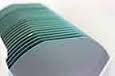
This unique structure dramatically reduces leakage current and parasitic capacitance while providing outstanding dimensional control during fabrication. The buried oxide layer also functions as a highly selective etch stop during Deep Reactive Ion Etching (DRIE), allowing engineers to manufacture suspended structures with excellent repeatability.
Today, SOI wafers are widely used for developing high-performance MEMS pressure sensors, RF switches, resonators, optical MEMS, inertial measurement units (IMUs), silicon photonic circuits, biosensors, and numerous semiconductor research devices requiring exceptional precision.
Fundamental Advantages of SOI Wafers for MEMS Fabrication
The growing adoption of Silicon-on-Insulator substrates is driven by several unique material properties that are difficult to achieve using conventional bulk silicon. These advantages simplify manufacturing while enabling smaller, faster, and more reliable MEMS devices.
Superior Electrical Isolation
The buried oxide (BOX) layer electrically separates the active silicon device layer from the handle wafer, minimizing current leakage and significantly reducing parasitic capacitance. This isolation improves sensor sensitivity, switching speed, signal integrity, and overall power efficiency. For RF MEMS devices and precision sensors, these electrical improvements directly translate into lower noise, faster response times, and greater measurement accuracy.
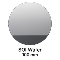
Compared to conventional silicon substrates, SOI technology can reduce parasitic capacitance by as much as 80%, making it particularly valuable for low-power electronics, RF communications, MEMS sensors, and high-frequency semiconductor devices.
Outstanding Mechanical Performance
The device layer consists of high-quality single-crystal silicon, providing excellent mechanical strength, low hysteresis, predictable elastic behavior, and exceptional fatigue resistance. These characteristics make SOI wafers ideal for fabricating movable MEMS structures such as cantilevers, membranes, springs, resonators, diaphragms, and micro-actuators that must maintain precise performance over billions of operating cycles.
Silicon's Young's Modulus of approximately 170 GPa provides excellent rigidity while maintaining relatively low mass, allowing engineers to design highly sensitive sensors capable of operating across broad frequency ranges.
Simplified MEMS Fabrication Using SOI Wafers
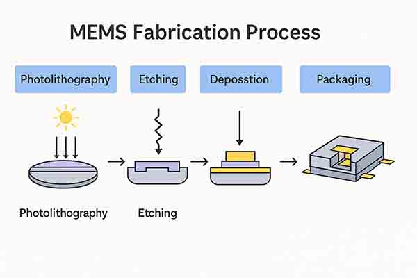
Beyond their superior electrical and mechanical properties, SOI wafers simplify many of the manufacturing steps required to fabricate MEMS devices. The buried oxide (BOX) layer performs multiple functions during processing, reducing fabrication complexity while improving yield and dimensional accuracy.
Instead of relying on complex endpoint detection methods during etching, engineers can use the buried oxide as a natural stopping layer. This improves manufacturing consistency and enables high-volume production of devices requiring micron-scale precision.
Major fabrication advantages of SOI substrates include:
- Natural etch-stop layer for Deep Reactive Ion Etching (DRIE)
- Excellent sacrificial layer for releasing suspended MEMS structures
- Superior electrical isolation without additional processing steps
- Highly uniform device-layer thickness across the entire wafer
- Compatibility with wafer bonding and three-dimensional MEMS architectures
- Improved fabrication repeatability for research and production
These advantages help researchers manufacture highly repeatable MEMS structures while reducing fabrication time and improving production yields. The ability to accurately define structural dimensions is particularly important for pressure sensors, resonators, accelerometers, gyroscopes, and RF MEMS switches, where even small dimensional variations can affect overall device performance.
UniversityWafer supplies research-grade silicon substrates and custom SOI wafers with a wide range of device-layer thicknesses, buried oxide thicknesses, crystal orientations, and resistivity options for universities, research laboratories, and semiconductor manufacturers worldwide.
Key Fabrication Technologies for SOI MEMS Devices
Several advanced semiconductor manufacturing techniques have been optimized specifically for Silicon-on-Insulator MEMS fabrication. These processes take full advantage of the unique SOI wafer structure to create miniature mechanical devices with exceptional precision and repeatability.
Deep Reactive Ion Etching (DRIE)
Deep Reactive Ion Etching (DRIE) is the primary micromachining technique used to manufacture modern MEMS devices. Unlike conventional plasma etching, DRIE creates deep, nearly vertical sidewalls while maintaining excellent dimensional accuracy.
Most MEMS manufacturers use the Bosch DRIE process, which alternates between silicon etching and sidewall passivation. This cyclic process produces high-aspect-ratio microstructures including cantilevers, diaphragms, comb drives, trenches, resonators, springs, and suspended beams.
The buried oxide layer inside an SOI wafer serves as an extremely selective etch stop. Once the plasma reaches the BOX layer, silicon removal effectively stops, allowing precise control over feature depth without damaging the handle wafer.
Typical DRIE Parameters for SOI MEMS Fabrication
| Parameter | Typical Value |
|---|---|
| Etch Rate | 2–10 μm/min |
| Aspect Ratio | Up to 30:1 |
| Sidewall Angle | 89–91° |
| Oxide Selectivity | Greater than 100:1 |
| Minimum Feature Size | Approximately 1–2 μm |
| Scallop Size | 50–500 nm |
DRIE has become indispensable for manufacturing MEMS pressure sensors, RF MEMS devices, inertial sensors, optical MEMS, biomedical devices, and silicon photonic structures requiring high-aspect-ratio features with exceptional dimensional accuracy.
Release of Suspended MEMS Structures
After patterning the silicon device layer, the buried oxide can be selectively removed to release movable MEMS components. This process transforms patterned silicon into free-standing cantilevers, membranes, bridges, diaphragms, comb drives, and resonators capable of mechanical movement.
Common release techniques include:
- Hydrofluoric Acid (HF) wet etching
- Vapor-phase HF etching
- Critical Point Drying (CPD)
- Anti-stiction surface treatments
- Supercritical drying techniques
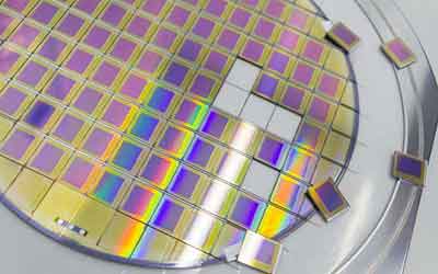
Carefully controlling the release process prevents stiction between movable structures and the substrate while preserving mechanical performance. Proper release techniques are essential for achieving high manufacturing yields in advanced MEMS devices.
Wafer Bonding Technologies
Many advanced MEMS devices require multiple wafers to be permanently joined together. SOI technology is fully compatible with several wafer bonding techniques that enable complex three-dimensional microsystems, wafer-level packaging, vacuum cavities, and integrated sensor platforms.
The most widely used bonding methods include:
- Anodic Bonding — Silicon bonded to glass using elevated temperature and electric fields for hermetic packaging.
- Fusion Bonding — Direct silicon-to-silicon or silicon-to-oxide bonding using atomically smooth surfaces and high-temperature annealing.
- Eutectic Bonding — Low-temperature metal-assisted bonding using materials such as gold-silicon (Au-Si).
- Adhesive Bonding — Polymer materials such as SU-8 or BCB provide strong mechanical bonding while minimizing thermal stress.
These bonding techniques enable the fabrication of pressure sensors, accelerometers, optical MEMS, microfluidic devices, resonators, RF MEMS switches, and biomedical microsystems that require enclosed cavities or stacked device architectures.
Researchers frequently combine silicon nitride coated wafers with SOI substrates to improve masking performance, dielectric isolation, chemical resistance, and mechanical durability during advanced semiconductor processing.
Advanced Applications of SOI Technology in MEMS Sensors
Modern Silicon-on-Insulator (SOI) wafers have enabled a new generation of MEMS sensors that combine outstanding mechanical performance with low power consumption and excellent electrical isolation. These advantages have made SOI substrates the preferred platform for manufacturing sensors used in consumer electronics, automotive safety systems, aerospace navigation, industrial automation, telecommunications, biomedical devices, and scientific instrumentation.
The combination of a high-quality silicon device layer and a buried oxide (BOX) layer allows engineers to fabricate highly sensitive mechanical structures while integrating electronic circuitry directly on the same substrate. This level of integration reduces package size, improves signal integrity, and increases long-term reliability.
Accelerometers and Gyroscopes
Accelerometers and gyroscopes are among the most common MEMS devices fabricated on SOI wafers. These sensors measure acceleration, vibration, tilt, and angular velocity for applications ranging from smartphones and gaming systems to aircraft navigation and autonomous vehicles.
Compared with conventional bulk silicon, SOI MEMS sensors offer several important advantages:
- Reduced parasitic capacitance for higher sensitivity
- Superior electrical isolation between sensing elements
- Excellent dimensional accuracy during fabrication
- Lower power consumption
- Higher resonant quality factors (Q)
- Improved long-term mechanical stability
- Excellent resistance to thermal drift
Today, billions of MEMS inertial sensors manufactured on SOI substrates are incorporated into smartphones, wearable devices, drones, robotics, industrial equipment, and advanced driver assistance systems (ADAS).
Pressure Sensors and MEMS Microphones
The excellent thickness uniformity of SOI wafers allows engineers to fabricate highly accurate silicon diaphragms for MEMS pressure sensors. Because diaphragm thickness directly determines sensor sensitivity, the exceptional uniformity of the SOI device layer results in highly repeatable device performance.
Common applications include:
- Automotive tire pressure monitoring systems (TPMS)
- Industrial pressure monitoring
- Medical pressure sensors
- Barometric sensors
- Flow sensors
- MEMS microphones
- Environmental monitoring systems
Benefits of SOI Wafers for Pressure Sensors
| Advantage | Benefit |
|---|---|
| Uniform Device Layer | Highly repeatable diaphragm thickness |
| BOX Layer | Excellent electrical isolation |
| Single-Crystal Silicon | Superior mechanical stability |
| CMOS Compatibility | Integrated signal conditioning electronics |
| Reduced Leakage Current | Lower power consumption |
MEMS microphones manufactured on SOI substrates also benefit from excellent acoustic performance, high signal-to-noise ratios, and compact package sizes that make them ideal for smartphones, hearing aids, voice assistants, and IoT devices.
RF MEMS Devices Built on SOI Wafers
As wireless communication systems continue moving toward higher frequencies, RF MEMS devices have become increasingly important for satellite communications, radar systems, 5G infrastructure, aerospace electronics, and defense applications.
The exceptional electrical isolation provided by SOI wafers minimizes signal losses while improving switching performance at microwave and millimeter-wave frequencies.
Common RF MEMS components include:
- RF switches
- Tunable capacitors
- High-Q resonators
- Bandpass filters
- Phase shifters
- Microwave relays
- Reconfigurable antennas
Researchers also utilize SOI wafers for RF transistors and fast switching devices that operate in demanding communication systems where minimizing insertion loss and maximizing isolation are critical design goals.
The reduced parasitic capacitance of SOI technology allows RF MEMS switches to achieve excellent linearity, faster switching speeds, lower insertion loss, and improved power handling compared to conventional semiconductor switching technologies.
Optical MEMS and Silicon Photonics
Another rapidly growing application of SOI technology is the development of optical MEMS (MOEMS) and silicon photonic integrated circuits. Because silicon has a much higher refractive index than silicon dioxide, SOI provides excellent optical confinement for integrated waveguides and photonic devices.
This unique optical property has made SOI wafers the industry standard for manufacturing silicon photonic circuits used in high-speed communications, optical sensing, quantum technologies, LiDAR systems, and data centers.
Micromirror Arrays and Optical Switching
SOI technology enables the fabrication of highly precise micromirror arrays capable of directing, modulating, or scanning light with exceptional accuracy. These devices are widely used in:
- LiDAR systems
- Digital Light Processing (DLP)
- Optical communications
- Adaptive optics
- Laser beam steering
- Optical cross-connect switches
- Biomedical imaging systems
The excellent mechanical stability of single-crystal silicon ensures long operating lifetimes while maintaining extremely accurate mirror positioning over billions of operating cycles.
Silicon Photonic Integrated Circuits
SOI wafers serve as the foundation for modern silicon photonics because the buried oxide layer confines light within silicon waveguides while minimizing optical losses. Engineers combine photonic components with MEMS actuators to manufacture tunable optical filters, optical switches, modulators, variable optical attenuators, interferometers, and optical phased arrays.
Advantages of SOI for Silicon Photonics
- Excellent optical confinement
- Low optical propagation loss
- Compact photonic circuit design
- Compatibility with CMOS semiconductor manufacturing
- High-speed optical communication
- Integration of electronics and photonics on one chip
UniversityWafer supplies SOI wafers for silicon photonics research with custom device-layer thicknesses, buried oxide layers, crystal orientations, and diameters for universities, research laboratories, and semiconductor manufacturers developing next-generation optical technologies.
Biomedical Applications of SOI MEMS Technology
Silicon-on-Insulator (SOI) wafers have become an essential platform for developing miniature biomedical devices that require exceptional precision, long-term reliability, and low power consumption. Their excellent electrical isolation and superior mechanical properties enable researchers to fabricate highly sensitive sensors capable of operating in demanding medical environments.
Today, SOI-based MEMS devices are widely investigated for implantable medical systems, diagnostic instruments, wearable healthcare devices, and point-of-care testing platforms. Their compatibility with CMOS electronics also allows sensing, signal processing, and wireless communication to be integrated onto a single chip.
Implantable MEMS Sensors
SOI substrates provide excellent stability for implantable MEMS devices that must operate reliably for years. Applications include:
- Blood pressure sensors
- Intracranial pressure monitoring
- Neural interfaces
- Drug delivery systems
- Implantable accelerometers
- Cardiovascular monitoring devices
- BioMEMS diagnostic sensors
When combined with suitable passivation layers such as silicon nitride, silicon dioxide, or biocompatible polymers, SOI MEMS devices demonstrate excellent long-term stability inside the human body.
Lab-on-a-Chip and Microfluidic Systems
Researchers also use SOI wafers to fabricate highly integrated lab-on-a-chip (LOC) and microfluidic devices. These miniature systems combine channels, valves, pumps, reaction chambers, and sensors on a single substrate, allowing complex laboratory analyses to be performed using only tiny sample volumes.
Typical applications include:
- DNA sequencing
- Protein analysis
- Cancer diagnostics
- Drug discovery
- Cell sorting
- Organ-on-chip research
- Point-of-care diagnostic systems
Researchers frequently combine SOI wafers with silicon nitride coated wafers to improve chemical resistance, dielectric isolation, and process compatibility during advanced microfabrication.
System-on-Chip (SoC) Integration Using SOI Technology
One of the greatest advantages of SOI technology is its compatibility with modern CMOS semiconductor manufacturing. Engineers can integrate MEMS sensors, analog circuitry, digital electronics, RF components, and communication interfaces onto a single semiconductor chip, reducing system complexity while improving performance.
Monolithic integration offers numerous advantages over assembling individual components after fabrication.
Benefits of SOI System-on-Chip Integration
| Integration Feature | System Benefit |
|---|---|
| Reduced Parasitic Effects | Higher signal integrity and lower electrical noise |
| Short Signal Paths | Improved speed and lower power consumption |
| Single-Chip Integration | Smaller package size and lower manufacturing cost |
| Improved Reliability | Fewer interconnect failures and simplified assembly |
| CMOS Compatibility | Easy integration of sensing and processing electronics |
These advantages have made SOI technology the preferred platform for smart sensors used in autonomous vehicles, industrial automation, aerospace systems, IoT devices, telecommunications, and wearable electronics.
Emerging Smart MEMS Systems
Modern SOI-MEMS devices increasingly incorporate artificial intelligence, wireless communication, and advanced signal processing directly on the sensor chip. These intelligent systems can perform self-calibration, real-time diagnostics, adaptive filtering, and predictive maintenance without requiring external processing hardware.
Applications include autonomous robots, environmental monitoring, industrial process control, smart factories, healthcare monitoring, and next-generation consumer electronics.
The Future of SOI Technology in MEMS Research
As semiconductor manufacturing continues to evolve, SOI technology is expected to play an even larger role in future MEMS development. Researchers are exploring thinner device layers, improved buried oxide materials, heterogeneous integration, and three-dimensional device architectures capable of combining mechanical, optical, electronic, and photonic functions on a single substrate.
Several important research directions include:
- Ultra-thin SOI wafers for nanoscale MEMS devices
- Artificial intelligence integrated directly into MEMS sensors
- Energy harvesting microsystems
- Quantum sensing technologies
- MEMS for silicon photonics and optical communications
- Advanced biomedical implants
- Three-dimensional semiconductor integration
- Flexible and wearable MEMS devices
These advances are expected to improve sensing accuracy, reduce power consumption, increase integration density, and enable entirely new classes of intelligent semiconductor devices.
Why Researchers Choose UniversityWafer SOI Wafers
UniversityWafer supplies high-quality Silicon-on-Insulator (SOI) wafers for universities, government laboratories, semiconductor manufacturers, and research organizations worldwide. Our SOI substrates are available in a wide range of diameters, crystal orientations, device-layer thicknesses, buried oxide (BOX) thicknesses, resistivity ranges, and doping configurations to support virtually every MEMS fabrication process.
Whether you are developing MEMS sensors, RF MEMS devices, silicon photonic circuits, pressure sensors, accelerometers, microfluidic systems, or biomedical microsystems, UniversityWafer can provide research-grade SOI substrates tailored to your application.
Conclusion
Silicon-on-Insulator technology has fundamentally transformed MEMS manufacturing by providing exceptional electrical isolation, precise dimensional control, and superior mechanical performance. These advantages allow researchers to fabricate smaller, faster, and more reliable semiconductor devices while simplifying many fabrication processes.
From RF MEMS and silicon photonics to biomedical sensors and autonomous vehicle technologies, SOI wafers continue to drive innovation across nearly every area of modern semiconductor research. As artificial intelligence, quantum technologies, advanced communications, and smart sensing systems continue to evolve, Silicon-on-Insulator substrates will remain one of the most important materials enabling the next generation of MEMS devices.
Related SOI & MEMS Resources
- Silicon-on-Insulator (SOI) Wafers – Learn about SOI wafer structures, buried oxide (BOX) layers, and custom specifications for semiconductor fabrication.
- SOI Wafer Technology – Explore the benefits of SOI substrates for low-power electronics, MEMS, and integrated circuits.
- SOI Transistors – Discover how Silicon-on-Insulator technology improves transistor performance and reduces parasitic capacitance.
- MEMS Wafers – Semiconductor substrates used to fabricate micro-electro-mechanical systems for sensing and actuation.
- Silicon Photonics – SOI substrates for waveguides, modulators, optical switches, and integrated photonic circuits.
- Silicon Wafers – Prime, test, and research-grade silicon wafers for MEMS, CMOS, and semiconductor manufacturing.
- Thermal Oxide Silicon Wafers – Silicon substrates with high-quality oxide layers for MEMS fabrication and dielectric isolation.
- Silicon Nitride Wafers – LPCVD and PECVD silicon nitride coatings for MEMS processing, masking, and dielectric applications.
- Young's Modulus of Silicon – Learn why silicon's mechanical properties are critical for MEMS beams, cantilevers, and resonators.
- Pressure Sensor Substrates – Materials used for MEMS pressure sensors, diaphragms, and sensing devices.
- Optical Device Substrates – Semiconductor wafers for optical MEMS, LiDAR, beam steering, and photonic systems.
- Research Substrates – Browse semiconductor wafers for MEMS, silicon photonics, RF devices, biomedical sensors, and advanced research.