Silicon-on-Insulator (SOI) Transistor
Learn how Silicon-on-Insulator (SOI) transistors and Fully Depleted SOI (FD-SOI) technology improve semiconductor performance through reduced leakage current, lower power consumption, and faster switching speeds. Discover SOI wafer structures, buried oxide (BOX) layers, transistor fabrication methods, common applications, and custom SOI wafers available for CMOS, MEMS, RF, photonics, and advanced semiconductor research.
Request a Fully Depleted SOI Wafer Quote
A Ph.D. researcher requested a custom Silicon-on-Insulator (SOI) wafer for fabricating a
Fully Depleted Silicon-on-Insulator (FD-SOI) transistor. The project required a thin silicon device layer,
a heavily doped handle wafer, and a thin buried oxide (BOX) layer suitable for advanced transistor research.
Research Request:
"I am trying to fabricate a fully depleted SOI transistor by utilizing the buried oxide layer as a bottom gate.
I need a degenerately doped silicon substrate with a thin buried oxide layer
(less than 300 nm). Ideally, the silicon device layer should be as thin as possible.
Since I am relatively new to SOI wafer processing, I would appreciate information regarding fabrication limits,
available wafer specifications, and whether this device concept is practical."
Reference #180855 for specifications and pricing.
Get Your SOI Wafer Quote FAST!
Or,
Buy Online
and Start Researching Today!
How Is a Fully Depleted SOI Transistor Fabricated?
A Fully Depleted Silicon-on-Insulator (FD-SOI) transistor is fabricated using a specialized
SOI wafer consisting of three primary layers:
- A thin crystalline silicon device layer
- A buried oxide (BOX) insulating layer
- A silicon handle substrate that provides mechanical support
Unlike conventional bulk CMOS technology, the transistor channel is formed within the ultra-thin silicon layer above the buried oxide.
Because the silicon layer is sufficiently thin, the channel becomes fully depleted during operation, reducing leakage current,
improving electrostatic control, and enabling lower operating voltages.
Typical FD-SOI Fabrication Process
- Select an SOI wafer with the desired silicon thickness, buried oxide thickness, and substrate doping.
- Grow or deposit the gate dielectric using thermal oxidation or atomic layer deposition.
- Deposit and pattern the gate electrode through photolithography and etching.
- Form the source and drain regions using ion implantation or epitaxial growth.
- Activate dopants with thermal annealing.
- Deposit dielectric layers and fabricate metal interconnects.
- Complete passivation and electrical testing.
The exact process flow depends on the target CMOS technology node, transistor geometry, and research objectives.
Researchers often customize the silicon thickness, buried oxide thickness, crystal orientation, and doping concentration
to optimize device performance.
Typical SOI Wafer Specifications for FD-SOI Research
| Parameter |
Typical Research Range |
| Silicon Device Layer |
5–100 nm (advanced) or thicker for research |
| Buried Oxide (BOX) |
20–300 nm |
| Wafer Diameter |
50 mm to 300 mm |
| Crystal Orientation |
(100) or (111) |
| Doping Type |
P-type or N-type |
| Surface Finish |
Single-side polished or double-side polished |
UniversityWafer supplies custom SOI wafers for
FD-SOI transistors, CMOS devices, MEMS fabrication, photonic integrated circuits, sensors, RF electronics,
and semiconductor research laboratories worldwide.
What Is a Fully Depleted SOI Transistor Used For?
A Fully Depleted Silicon-on-Insulator (FD-SOI) transistor is designed for semiconductor devices that require low power consumption, fast switching, reduced leakage current, and precise control of the transistor channel. In an FD-SOI structure, the thin silicon device layer above the buried oxide is fully depleted of mobile charge carriers during operation, helping reduce short-channel effects and improve electrostatic control.
FD-SOI technology is commonly considered for applications where designers need to balance performance, energy efficiency, reliability, and compact device dimensions.
Common FD-SOI Applications
-
Low-Power Electronics: FD-SOI transistors are used in battery-powered devices such as wearables, portable electronics, sensors, and Internet of Things devices. Reduced leakage current and lower operating voltages can help extend battery life.
-
Mobile and Embedded Processors: FD-SOI can support processors and system-on-chip designs that require fast switching while maintaining low power consumption. This makes the technology useful for mobile, embedded, and edge-computing applications.
-
Automotive Electronics: FD-SOI technology can be used in automotive processors, sensors, control systems, and mixed-signal circuits. Its low leakage and resistance to certain radiation-induced effects can be beneficial in demanding operating environments.
-
Aerospace and Radiation-Sensitive Devices: The insulating buried oxide layer helps isolate the active device region from the bulk substrate. This structure may improve resistance to some radiation-related effects, making SOI technology valuable for aerospace and high-reliability electronics.
-
RF and Communication Systems: FD-SOI platforms can support radio-frequency, wireless, and communication circuits that require low parasitic capacitance, high switching speed, and efficient power management.
-
Analog and Mixed-Signal Circuits: FD-SOI transistors can provide good threshold-voltage control and reduced substrate interference. These properties are useful in analog-to-digital converters, digital-to-analog converters, sensor interfaces, and other mixed-signal devices.
-
Imaging and Photodetector Systems: Specialized SOI wafers may be used to integrate transistors with photodiodes, image sensors, and other optoelectronic components on a common substrate.
Integrating a Photodiode with a Fully Depleted SOI Transistor
Integrating a photodiode with an FD-SOI transistor may allow the light-sensing element and its associated control or readout circuitry to be fabricated within the same device architecture. The required SOI wafer specifications depend on the photodiode design, absorption depth, electrical isolation requirements, and transistor process.
Important wafer parameters may include:
- Top silicon thickness
- Buried oxide thickness
- Device-layer doping concentration
- Handle-wafer resistivity and doping type
- Wafer diameter
- Surface orientation
- Single-BOX or double-BOX construction
- Epitaxial layer thickness and doping
Example SOI Wafer Request for Photodiode Integration
An engineer developing a novel imaging technology requested SOI wafer options for photodiode and FD-SOI transistor research.
The project currently uses silicon wafers with highly doped epitaxial layers approximately 200 nm to 600 nm thick. During initial testing, the base wafer primarily serves as mechanical support, so the handle-wafer specifications remain flexible.
The engineer also requested information about integrating a novel photodiode with a fully depleted SOI transistor using SOITEC UNIBOND and Smart Cut SOI wafers.
The requested structure included a buried oxide layer of approximately 25 nm and a top silicon device layer between approximately 600 nm and 1,500 nm.
The researcher was also interested in determining whether double-BOX SOI wafers could be supplied, with the second oxide layer serving as a process stop or isolation layer. Initial quantities were expected to be approximately 25 to 50 wafers for research and development.
Reference #266339 for specifications and pricing.
Fully Depleted SOI Transistor Structure
The diagram below illustrates the primary layers and electrical terminals in a simplified FD-SOI transistor structure.
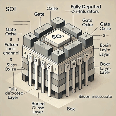
FD-SOI Transistor Diagram Labels
-
Gate: The control electrode that regulates the electrical conductivity of the transistor channel.
-
Gate Oxide: A thin dielectric layer that electrically isolates the gate from the silicon channel.
-
Fully Depleted Channel: The region between the source and drain through which current flows when the transistor is switched on. The thin device layer allows the channel to become fully depleted during operation.
-
Source: The terminal through which charge carriers enter the transistor channel.
-
Drain: The terminal through which charge carriers leave the transistor channel.
-
Silicon Device Layer: The thin crystalline silicon film above the buried oxide where the transistor channel, source, and drain are formed.
-
BOX Layer: The buried oxide layer electrically isolates the active silicon device layer from the handle substrate and reduces parasitic capacitance.
-
Silicon Handle Substrate: The bulk silicon wafer beneath the buried oxide that provides mechanical support and may also be used for back-gate or body-bias control in some device structures.
SOI Wafer Specifications for FD-SOI Research
Researchers selecting an SOI wafer for transistor fabrication should specify the device-layer thickness, buried oxide thickness, doping type, resistivity, crystal orientation, wafer diameter, surface finish, and required thermal budget.
Thin device layers are generally preferred for fully depleted transistor structures because the silicon film must be thin enough for the channel to become fully depleted. However, the correct thickness depends on the transistor geometry, doping concentration, operating voltage, and fabrication process.
UniversityWafer supplies SOI substrates for transistor, photodiode, sensor, MEMS, CMOS, and semiconductor research. Custom and research-grade specifications may be available depending on diameter, device-layer thickness, buried oxide thickness, and quantity.
Related SOI and Semiconductor Resources
