
What Is Vacuum Thin-Film Deposition?
Vacuum thin-film deposition is the controlled formation of a thin layer of material on a substrate inside a low-pressure or vacuum environment. Depending on the process and application, deposited films can range from only a few nanometers to several micrometers in thickness.
Thin films are essential in semiconductor manufacturing, MEMS, sensors, photonics, solar cells, RF electronics, optical coatings, and advanced materials research. Researchers commonly deposit films onto silicon wafers, glass wafers, fused silica wafers, sapphire, quartz, and other engineered substrates.
What Materials Can Be Deposited as Thin Films?
Thin-film deposition processes can create conductive, insulating, optical, semiconducting, magnetic, and protective coatings. The appropriate material depends on the electrical, optical, mechanical, and chemical requirements of the final device.
- Metals: aluminum, copper, titanium, chromium, nickel, gold, platinum, tungsten, molybdenum, and other conductive materials
- Dielectrics: silicon dioxide (SiO2), silicon nitride (Si3N4), and other insulating films
- Semiconductors: silicon, germanium, and selected compound semiconductor materials
- Optical Films: reflective, anti-reflective, interference, and protective coatings
- Functional Films: adhesion layers, diffusion barriers, seed layers, electrodes, and passivation coatings
What Are the Main Thin-Film Deposition Methods?
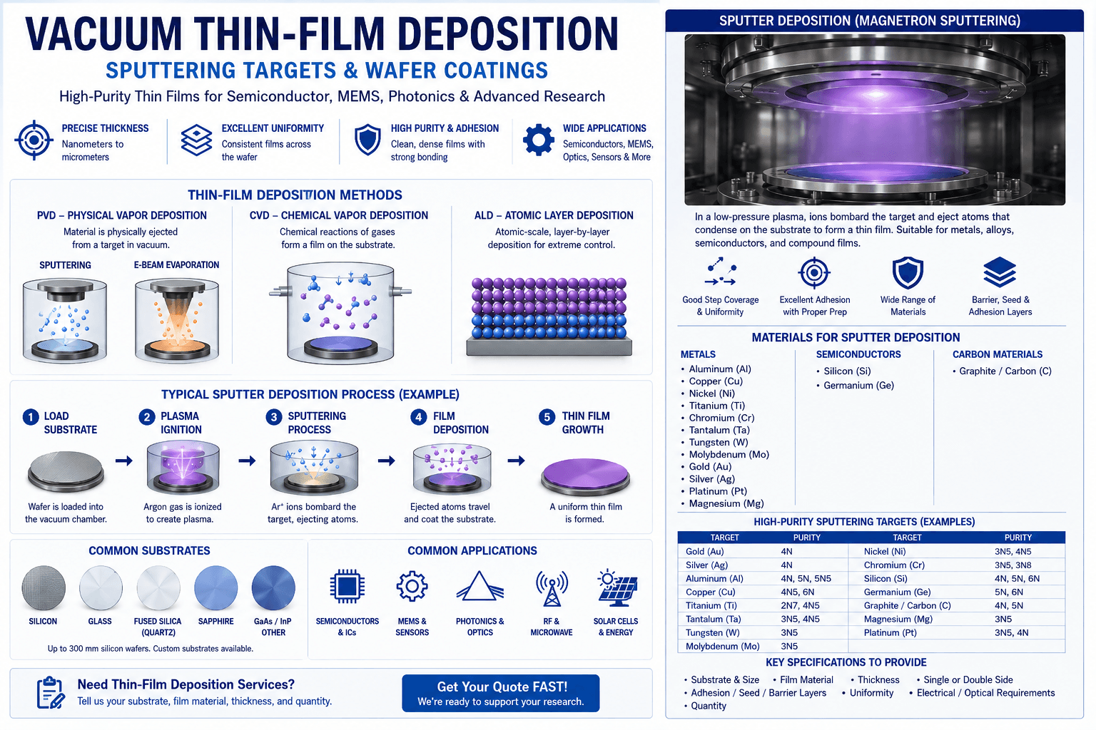
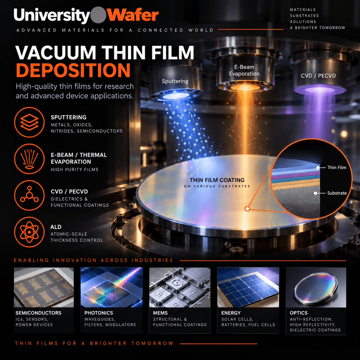
Thin-film deposition methods are commonly grouped into physical vapor deposition (PVD) and chemical vapor deposition (CVD). Other important processes, such as atomic layer deposition (ALD), are also widely used when extremely conformal and precisely controlled films are required.
Physical Vapor Deposition (PVD)
Physical vapor deposition transfers material from a solid source to the substrate through a vacuum environment. Common PVD techniques include sputtering and electron-beam evaporation.
PVD is commonly used to deposit metals, adhesion layers, conductive films, optical coatings, and barrier layers on semiconductor and research substrates.
Sputter Deposition
In sputtering, energetic ions bombard a solid target and eject atoms from its surface. These atoms travel through the vacuum chamber and condense on the wafer or substrate to form a thin film.
Sputtering is widely used for metal deposition, dielectric coatings, seed layers, barrier layers, reflective coatings, and other thin-film applications where good film adhesion and uniformity are required.
Electron-Beam Evaporation
In electron-beam evaporation, a focused electron beam heats the source material until it evaporates. The vapor then condenses on the substrate.
Because evaporation is relatively directional, it is often useful for applications such as patterned metal deposition and lift-off processing.
Chemical Vapor Deposition (CVD)
Chemical vapor deposition forms thin films through chemical reactions involving gaseous precursors at or near the substrate surface.
CVD is widely used in semiconductor fabrication for films such as TEOS silicon dioxide, silicon nitride, polysilicon, and other dielectric or semiconductor layers.
Why Use Vacuum for Thin-Film Deposition?
A controlled vacuum environment reduces unwanted gas-phase collisions and contamination while allowing deposition conditions to be precisely managed. This can improve repeatability, purity, and control over film thickness and microstructure.
Depending on the deposition method, vacuum processing can help provide:
- Controlled film thickness
- Improved film purity
- Good thickness uniformity
- Repeatable electrical properties
- Controlled optical properties
- Strong film-to-substrate adhesion
- Compatibility with semiconductor fabrication
Thin-Film Deposition on Silicon Wafers
Silicon wafers are among the most widely used thin-film deposition substrates because they provide a flat, well-characterized surface compatible with semiconductor processing.
Thin films deposited on silicon can serve as electrical contacts, dielectric layers, diffusion barriers, optical layers, sensing surfaces, structural films, or processing layers used during device fabrication.
When ordering silicon wafers for deposition, researchers may need to specify diameter, thickness, crystal orientation, resistivity, dopant type, surface finish, oxide thickness, and total thickness variation (TTV).
Thin Films on Glass, Quartz, and Fused Silica
Transparent substrates are important for photonics, optical coatings, sensors, displays, and microfluidic applications. Glass wafers and fused silica wafers can be coated with conductive, reflective, dielectric, or optical thin films depending on the device requirements.
Substrate composition, surface roughness, thermal expansion, transparency, and process temperature should all be considered when selecting a non-silicon substrate for deposition.
Thin-Film Deposition for MEMS and Sensors
Thin films are fundamental to MEMS fabrication and sensor manufacturing. Deposited materials can function as electrodes, piezoresistive layers, dielectric films, structural layers, protective coatings, and sensing surfaces.
In many MEMS processes, thin-film deposition is combined with photolithography, etching, wafer bonding, oxidation, and micromachining to build multilayer microstructures.
Thin-Film Deposition for Photonics and Optics
Thin films are widely used to control reflection, transmission, absorption, and phase in optical devices. Applications include mirrors, filters, anti-reflection coatings, photonic devices, optical sensors, and spectroscopic components.
Film thickness and refractive index are especially important in optical applications because even small deviations can change the spectral response of a multilayer coating.
Thin-Film Deposition for Solar Cells and Energy Devices
Thin-film processing is also used in photovoltaic and energy research for contacts, transparent conductive layers, passivation films, barrier layers, absorbers, and device interfaces.
Researchers may use deposition techniques such as sputtering, evaporation, CVD, or ALD depending on the required material, temperature limit, film thickness, and device architecture.
What Specifications Matter for a Thin-Film Deposition Quote?
To receive an accurate thin-film deposition quote, provide as many process details as possible. Important specifications may include:
- Substrate material – silicon, glass, fused silica, sapphire, quartz, or other material
- Wafer diameter or substrate dimensions
- Substrate thickness
- Film material
- Required film thickness
- Deposition method – sputtering, e-beam evaporation, CVD, or other process
- Single-side or double-side deposition
- Adhesion or seed-layer requirements
- Thickness uniformity requirements
- Quantity
Common Thin-Film Deposition Applications
- Integrated circuit fabrication
- MEMS and microsensors
- RF and microwave devices
- Photonic devices
- Optical coatings
- Solar cells and photovoltaics
- Biomedical sensors
- Electrodes and contact metals
- Barrier and adhesion layers
- Thin-film materials research
Need Thin-Film Deposition or Wafer Coating Services?
UniversityWafer, Inc. supports research and development projects requiring sputtered metals, dielectric films, semiconductor coatings, optical layers, and custom wafer processing on silicon, glass, fused silica, sapphire, and other substrate materials.
Get Your Thin-Film Deposition Quote FAST!
Or, Buy Wafers Online
and Start Researching Today!
What Is Sputter Deposition?
Sputter deposition is a physical vapor deposition (PVD) technique used to form thin films on silicon wafers, glass, fused silica, sapphire, and other substrates. It is widely used for semiconductor metallization, MEMS, sensors, RF devices, optical coatings, solar cells, electrodes, barrier layers, and materials research.
During sputtering, a low-pressure process gas—commonly argon—is introduced into a vacuum chamber and ionized to form a plasma. Positively charged ions from the plasma are accelerated toward a negatively biased sputtering target. Ion bombardment transfers momentum to atoms in the target, causing some of them to be ejected from the target surface.
The sputtered species travel through the chamber and condense on the substrate, gradually forming a thin film. Film properties depend on factors such as target material, gas pressure, applied power, substrate temperature, target-to-substrate geometry, deposition rate, and substrate preparation.
What Is Magnetron Sputtering?
Magnetron sputtering is a widely used form of sputter deposition in which magnetic fields help confine electrons near the target surface. This increases the probability of collisions between electrons and process-gas atoms, helping sustain a dense plasma near the target.
Magnetron sputtering can provide practical deposition rates while maintaining the low-pressure environment needed for controlled thin-film growth. It is commonly used to deposit metals, alloys, semiconductors, and compound films for research and industrial applications.
DC vs. RF Sputtering
The electrical properties of the target material help determine which sputtering technique is appropriate.
DC Sputtering
Direct-current (DC) sputtering is commonly used with electrically conductive targets such as aluminum, copper, titanium, chromium, nickel, platinum, and gold. A DC potential maintains the target at a negative electrical potential relative to the plasma.
RF Sputtering
Radio-frequency (RF) sputtering can be used for insulating as well as conductive target materials. The alternating electric field helps prevent the persistent surface charging that would interfere with conventional DC sputtering of an insulating target.
RF sputtering is therefore useful for depositing certain dielectric, ceramic, and compound thin films in addition to conductive materials.
What Is Reactive Sputtering?
Reactive sputtering introduces a reactive gas, such as oxygen or nitrogen, in addition to an inert sputtering gas. The sputtered material reacts with the gas to form a compound film on the substrate.
For example, reactive sputtering can be used to form selected metal oxides, nitrides, and other compound coatings. Process control is important because reactive-gas flow can affect target-surface chemistry, deposition rate, film composition, and electrical or optical properties.
Sputtered Films on Silicon Wafers
Silicon wafers provide a flat, well-characterized substrate for sputtered metals, semiconductors, dielectrics, and compound films.
UniversityWafer can support coated silicon wafers up to 300 mm in diameter, depending on the requested material, equipment, and process requirements.
Before deposition, wafer specifications such as surface finish, oxide thickness, resistivity, crystal orientation, cleanliness, and substrate temperature limits should be considered because they can influence the film/substrate interface and subsequent device processing.
Sputtering on Glass, Quartz, Fused Silica, and Sapphire
Sputtering is not limited to silicon. Thin films can also be deposited on fused silica wafers, glass wafers, quartz, sapphire, and other compatible substrates.
These substrate systems are useful for optical coatings, transparent devices, sensors, photonics, microfluidics, electrodes, and materials research. Substrate temperature limits, thermal expansion, surface chemistry, roughness, and optical properties should be considered when developing the deposition process.
Sputtering vs. E-Beam Evaporation
Both sputtering and electron-beam evaporation are PVD techniques, but they transport material to the substrate differently.
E-beam evaporation heats a source material until it evaporates and produces a comparatively directional vapor flux. Sputtering ejects atoms from a target through energetic ion bombardment, and gas-phase scattering can make the arriving flux less directional than typical evaporation.
As a result, sputtering can provide useful coverage over surface topography, while the more directional nature of evaporation can be advantageous for some lift-off lithography processes.
This does not mean sputtering cannot be used with lift-off. Successful sputter lift-off is possible, but resist profile, feature geometry, film thickness, chamber pressure, deposition geometry, and sidewall coating must be carefully controlled to avoid continuous film formation across the resist sidewalls.
Film Adhesion and Surface Preparation
Good thin-film adhesion depends on both the deposited material and the substrate surface. Particles, organic contamination, adsorbed moisture, and native surface layers can affect the film/substrate interface.
Depending on the process, substrate preparation may include solvent cleaning, dehydration, plasma treatment, or an in-situ sputter clean immediately before deposition. The appropriate method depends on the substrate, film material, and required interface properties.
For silicon, removal of native SiO2 may be desirable when a low-resistance metal-to-silicon contact is required. In other applications, however, the oxide is intentionally retained because it provides electrical insulation or forms part of the device structure.
Therefore, treatments such as an HF-based oxide-removal step should only be specified when they are compatible with the intended device and process flow.
Adhesion, Seed, and Barrier Layers
Many thin-film stacks contain more than one material. An intermediate layer can be added to improve adhesion, provide a conductive seed surface, or limit diffusion between materials.
- Adhesion layers can improve bonding between a deposited film and the underlying substrate.
- Seed layers provide a conductive or crystallographically useful starting surface for subsequent deposition or electroplating.
- Diffusion barriers help limit interdiffusion or chemical interaction between adjacent materials.
Titanium and chromium are commonly used as adhesion layers in selected metal stacks, while tantalum and related materials are used in some diffusion-barrier applications. The correct stack depends on the substrate, deposited material, temperature, and device requirements.
Materials Used for Sputter Deposition
A wide range of materials can be sputtered. They should be categorized by material type rather than treating every sputtering target as a metal.
Metal Sputtering Targets
- Aluminum (Al)
- Copper (Cu)
- Nickel (Ni)
- Titanium (Ti)
- Chromium (Cr)
- Tantalum (Ta)
- Tungsten (W)
- Molybdenum (Mo)
- Gold (Au)
- Silver (Ag)
- Platinum (Pt)
- Magnesium (Mg)
Semiconductor and Carbon Targets
- Silicon (Si)
- Germanium (Ge)
- Graphite / Carbon (C)
What Does Sputtering Target Purity Mean?
Sputtering-target purity is often expressed using an "N" notation. For example, 4N corresponds nominally to 99.99% purity, while 5N corresponds nominally to 99.999% purity.
Higher target purity can be important when trace impurities could affect electrical, optical, magnetic, or semiconductor properties. However, target purity alone does not determine final film purity. Chamber background, process gases, target conditioning, substrate cleanliness, and deposition-system history can also introduce impurities.
High-Purity Sputtering Targets
The following sputtering target materials are available for vacuum thin-film deposition, semiconductor research, optical coatings, metallization, and materials-development projects.
| Sputtering Target | Purity | Image |
|---|---|---|
| Gold (Au) Target | 4N |  |
| Silver (Ag) Target | 4N |  |
| Platinum (Pt) Target | 3N5, 4N |  |
| Aluminum (Al) Target | 4N, 5N, 5N5 |  |
| Copper (Cu) Target | 4N5, 6N |  |
| Titanium (Ti) Target | 2N7, 4N5 |  |
| Nickel (Ni) Target | 3N5, 4N5 |  |
| Tantalum (Ta) Target | 3N5, 4N5 |  |
| Tungsten (W) Target | 3N5 |  |
| Molybdenum (Mo) Target | 3N5 |  |
| Silicon (Si) Target | 4N, 5N, 6N |  |
| Graphite / Carbon (C) Target | 4N, 5N |  |
| Chromium (Cr) Target | 3N5, 3N8 |  |
| Magnesium (Mg) Target | 3N5 |  |
| Germanium (Ge) Target | 5N, 6N |  |
How Do I Choose a Sputtering Target?
Target selection depends on the film composition and the performance requirements of the finished device. Important specifications can include:
- Target material and composition
- Purity
- Target diameter and thickness
- Target geometry
- Backing plate requirements
- Bonding method
- Deposition system compatibility
- Required film composition and properties
For alloy or compound targets, composition and homogeneity can also be important because the deposited film may need to meet specific electrical, optical, mechanical, or chemical requirements.
What Specifications Matter for Sputter Deposition?
When requesting sputtered films, provide as much information about the desired film and substrate as possible. Useful specifications include:
- Substrate material
- Wafer diameter or substrate dimensions
- Film material
- Required film thickness
- Thickness uniformity requirements
- Single-side or double-side coating
- Adhesion, seed, or barrier layers
- Electrical or optical requirements
- Patterned or blanket deposition
- Quantity
Providing the complete film stack—for example, Si / SiO2 / Ti / Au with individual layer thicknesses—is more useful than requesting only "gold-coated silicon."
Common Applications of Sputtered Thin Films
- Semiconductor metallization
- MEMS and microsensors
- Electrical contacts and electrodes
- RF and microwave devices
- Diffusion barriers
- Adhesion and seed layers
- Optical and reflective coatings
- Solar-cell research
- Photonic devices
- Thin-film materials research
Need Sputtered Thin Films or Sputtering Targets?
Submit your substrate material, wafer size, target or film material, required film thickness, layer stack, and quantity so the appropriate sputtering process and materials can be evaluated.