Substrates for Wafer Fabrication
UniversityWafer supplies semiconductor substrates, epitaxial wafers, coated wafers, and custom layer structures
for wafer fabrication, microelectronics, photonics, MEMS, sensors, RF devices, and compound-semiconductor research.
Researchers can request wafers based on substrate material, diameter, crystal orientation, thickness, conductivity type,
resistivity, surface finish, epitaxial composition, doping, and film thickness.
Research Example: InGaAs on InP Epitaxial Wafers
A wafer fabrication engineer from a domestic Microelectronics Center requested a quotation for a custom
InGaAs epitaxial wafer
structure for microelectronic device research.
Requested wafer specifications:
-
Epitaxial material: In0.53Ga0.47As
-
Substrate:
InP:Fe (111B)
- Wafer diameter: 2 inches
- Substrate thickness: 350 ±25 µm
- Surface finish: Both sides polished
- Edge configuration: Two EJ flats
- Epitaxial thickness: 0.5 µm
- Conductivity: n-type, silicon-doped
- Target resistivity: greater than 13 Ω·cm
UniversityWafer Response
UniversityWafer can supply In0.53Ga0.47As epitaxial layers grown on InP substrates using
MOCVD epitaxy.
This composition is commonly selected because it is approximately lattice matched to indium phosphide, helping reduce
strain and crystal defects in the epitaxial layer.
Available doping options may include:
- Undoped or unintentionally doped InGaAs
- Silicon-doped n-type InGaAs
- Zinc-doped p-type InGaAs
InGaAs layers with different indium-to-gallium ratios may also be possible. However, compositions that are not lattice
matched to InP can introduce strain, which may affect crystal quality, interface performance, carrier mobility, and
device behavior.
For this research example, fabrication was available on 2-inch and 3-inch InP substrates. Availability on other wafer
diameters depends on the requested layer structure, substrate orientation, doping, thickness, and production capability.
Epitaxial wafer pricing depends on substrate specifications, wafer diameter, epi-layer composition, doping,
target thickness, characterization requirements, and quantity. Thicker epitaxial layers generally increase growth time
and total fabrication cost.
Reference #131300 when requesting related specifications and pricing.
Available Wafer Fabrication Substrates
UniversityWafer supplies materials for semiconductor process development, university cleanrooms, pilot production,
device prototyping, thin-film deposition, wafer bonding, lithography, etching, oxidation, and epitaxial growth.
-
Silicon wafers
for ICs, MEMS, sensors, oxidation, diffusion, implantation, and thin-film deposition
-
Silicon-on-insulator wafers
for MEMS, photonics, RF, CMOS, and low-power device research
-
Silicon epitaxial wafers
with controlled epi thickness, resistivity, and dopant profiles
-
Gallium arsenide wafers
for RF, microwave, photonics, LEDs, and high-speed electronics
-
Indium phosphide wafers
for InGaAs epitaxy, photodetectors, lasers, and high-frequency devices
-
GaN on sapphire wafers
for LEDs, HEMTs, UV detectors, and nanophotonic devices
-
Silicon carbide wafers
for high-temperature, high-voltage, and power-device fabrication
-
Sapphire wafers
for epitaxy, optical devices, dielectric substrates, and high-temperature processing
-
Fused silica and glass wafers
for microfluidics, optics, wafer bonding, and sensor fabrication
Custom Coated and Epitaxial Wafers
Custom wafers may be supplied with deposited, grown, or bonded layers according to the requirements of your fabrication
process. Available options may include:
Information Needed for a Wafer Fabrication Quote
To receive an accurate recommendation and quotation, include as many of the following specifications as possible:
- Substrate material
- Wafer diameter and thickness
- Crystal orientation
- Dopant and conductivity type
- Target resistivity or carrier concentration
- Single-side or double-side polish
- Epitaxial or deposited film material
- Film thickness and composition
- Refractive index, stress, or roughness requirements
- Flatness, bow, warp, and TTV limits
- Required characterization data
- Quantity and delivery requirements
Get Your Wafer Fabrication Quote FAST! or
buy available wafers online
and start researching today.
What Is Wafer Fabrication?
Wafer fabrication is the sequence of semiconductor manufacturing processes used to build electronic,
photonic, MEMS, sensor, and power devices on a wafer substrate. Fabrication begins with a carefully selected
semiconductor wafer
and may involve repeated cycles of cleaning, oxidation, thin-film deposition, photolithography, etching, doping,
annealing, metallization, and surface characterization.
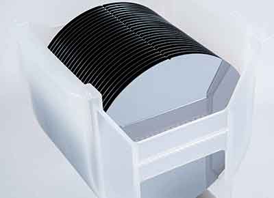 The purpose of the wafer fabrication process is to form precisely controlled material layers and microscopic device
structures on the wafer surface. Depending on the application, a process flow may produce integrated circuits,
transistors, photodetectors, LEDs, MEMS devices, microfluidic systems, solar cells, or photonic components.
The purpose of the wafer fabrication process is to form precisely controlled material layers and microscopic device
structures on the wafer surface. Depending on the application, a process flow may produce integrated circuits,
transistors, photodetectors, LEDs, MEMS devices, microfluidic systems, solar cells, or photonic components.
Although silicon wafers
are the most widely used substrates, fabrication processes may also use silicon-on-insulator, silicon carbide,
gallium arsenide, gallium nitride, indium phosphide, sapphire, glass, quartz, and other research materials.
Core Wafer Fabrication Process Steps
A semiconductor wafer may pass through hundreds of individual operations before the completed devices are tested
and separated. The exact sequence depends on the device design, substrate material, layer structure, critical
dimensions, thermal budget, and production requirements.
-
Wafer selection and preparation:
The substrate is selected according to diameter, orientation, thickness, conductivity type, dopant,
resistivity, surface finish, flatness, and device requirements.
-
Wafer cleaning:
Organic residue, metallic contamination, particles, and native oxide are removed before high-temperature
processing or thin-film deposition.
-
Thermal oxidation:
Silicon may be exposed to oxygen or water vapor at elevated temperatures to grow a controlled silicon dioxide
layer. Researchers can also purchase
thermal oxide wafers
with specified oxide thicknesses.
-
Thin-film deposition:
Dielectric, semiconductor, and metal films may be deposited using LPCVD, PECVD, ALD, sputtering,
evaporation, MOCVD, or other deposition methods.
-
Photolithography:
A light-sensitive photoresist is applied, exposed through a photomask, and developed to transfer a pattern
onto the wafer. Learn more about
photolithography.
-
Etching:
Unprotected material is removed using wet chemical etching, plasma etching, reactive-ion etching, or deep
reactive-ion etching. See
silicon wafer etching methods.
-
Doping and ion implantation:
Dopant atoms are introduced to modify the electrical conductivity of selected regions. The required
doping concentration
depends on the device structure.
-
Annealing:
Thermal processing activates implanted dopants, repairs crystal damage, densifies films, or modifies
interfaces and material properties.
-
Metallization:
Conductive layers are patterned to form contacts, electrodes, interconnects, bond pads, gates, and device wiring.
-
Passivation and packaging preparation:
Protective dielectric layers may be added before electrical testing, wafer dicing, bonding, and packaging.
Thin-Film Deposition in Semiconductor Manufacturing
Thin-film deposition allows researchers and manufacturers to control the electrical, optical, chemical,
and mechanical properties of a wafer surface. Common deposited materials include silicon dioxide,
silicon nitride, polysilicon, aluminum oxide, metals, compound semiconductors, and epitaxial device layers.
-
LPCVD: Low-Pressure Chemical Vapor Deposition is commonly used for stoichiometric silicon nitride,
polysilicon, and other uniform films. See
LPCVD deposition.
-
PECVD: Plasma-Enhanced Chemical Vapor Deposition permits lower-temperature deposition of
silicon dioxide, silicon nitride, and related films.
-
ALD: Atomic Layer Deposition provides highly conformal, thickness-controlled films for
high-k dielectrics, passivation, sensors, and nanoscale structures.
-
MOCVD: Metal-Organic Chemical Vapor Deposition is widely used for compound-semiconductor
epitaxy, including GaN, GaAs, InP, and InGaAs structures. Learn about
MOCVD epitaxy.
-
PVD: Physical Vapor Deposition methods such as sputtering and evaporation are commonly used
to deposit metals and functional coatings.
Photolithography and Pattern Transfer
Photolithography defines the microscopic geometry of a semiconductor device. A wafer is coated with photoresist,
aligned with a photomask, exposed to ultraviolet light, and developed to reveal selected areas of the underlying
film. The resulting resist pattern protects portions of the wafer during etching, implantation, deposition,
or lift-off.
Complex integrated circuits require many lithography cycles. Each layer must be accurately aligned with the
previous pattern, making wafer flatness, surface quality, particle control, resist adhesion, and exposure accuracy
important parts of the fabrication process.
Etching Methods Used in Wafer Fabrication
Etching removes selected material after lithographic patterning. The process must provide the required etch rate,
selectivity, sidewall profile, uniformity, and surface condition.
-
Wet etching: Uses liquid chemical solutions and is often economical for oxide removal,
wafer cleaning, crystal-orientation-dependent silicon etching, and bulk micromachining.
-
Dry etching: Uses reactive gases or plasma to produce more directional features and smaller
geometries.
-
Reactive-ion etching: Combines physical ion bombardment with chemical reactions to achieve
controlled feature profiles.
-
Deep reactive-ion etching: Creates deep, high-aspect-ratio structures for MEMS,
microfluidics, through-silicon vias, and advanced sensor fabrication.
Fabricating Integrated Circuits and Microelectronic Devices
Integrated circuits are fabricated by repeatedly forming and patterning insulating, semiconducting, and conductive
layers. Silicon is widely used because its electrical properties can be controlled through doping and because it
forms a stable native oxide that is valuable for insulation, masking, passivation, and transistor fabrication.
Unlike a metal conductor, intrinsic silicon is a semiconductor. Its conductivity can be adjusted by introducing
controlled concentrations of donor or acceptor dopants. Researchers often select wafers according to
silicon resistivity,
dopant type, crystal orientation, oxygen content, and surface finish.
Wafer-fabricated microelectronic devices include:
- CMOS integrated circuits
- MOSFETs and power transistors
- Diodes and rectifiers
- MEMS sensors and actuators
- Photodiodes and image sensors
- RF and microwave devices
- Microprocessors and memory devices
- Solar cells and photovoltaic devices
Research Example: Custom LPCVD Silicon Nitride Wafer
A postdoctoral researcher requested a customized wafer structure for optical-device fabrication. The required
silicon nitride layer needed to be stoichiometric
LPCVD silicon nitride
with a refractive index of approximately 2 in the visible wavelength range.
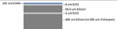
Custom coated wafers may require specifications for wafer diameter, substrate orientation, silicon resistivity,
nitride stoichiometry, film stress, refractive index, film thickness, surface roughness, edge exclusion,
and single- or double-side deposition.
Reference #254398 when requesting related specifications and pricing.
Silicon Wafer Kerf Loss During Manufacturing
Kerf loss is the material removed by a cutting wire, saw blade, laser, or abrasive process when
an ingot, wafer, die, or substrate is sliced. In silicon wafer manufacturing, kerf material may consist of fine
silicon particles mixed with cutting fluid, abrasive material, metal contamination, or other process residue.
Kerf loss is especially important in
solar wafer manufacturing
because raw silicon contributes substantially to production cost. The percentage of material lost is not fixed.
It varies according to:
- Ingot diameter and geometry
- Target wafer thickness
- Wire diameter or blade width
- Slicing method and equipment generation
- Feed rate and cutting conditions
- Wafer breakage and downstream yield
- Whether reusable edge material is included in the calculation
Estimates such as 30% or 40% may be reasonable for particular production assumptions, but they should not be
presented as universal industry values. Modern manufacturers reduce material loss through thinner cutting wires,
optimized slurry systems, diamond-wire sawing, thinner wafers, improved process control, and higher wafer yield.
Can Silicon Kerf Waste Be Recycled?
Some silicon kerf can be recovered, but the practicality of recycling depends on purity, particle size,
contamination, collection method, processing cost, and the quality required for the final application.
Recovery may involve:
- Separating silicon particles from cutting fluids or slurry
- Removing metal and abrasive contamination
- Chemical purification
- Thermal treatment or remelting
- Reusing recovered silicon in lower-purity applications
- Converting silicon waste into powders or specialty materials
Recycling practices differ between manufacturers. It would therefore be inaccurate to state that every solar
manufacturer recycles all kerf waste. A reliable industry estimate should define the wafer technology,
manufacturing region, cutting method, time period, contamination level, and whether the calculation measures
internal reuse, third-party recycling, downcycling, or disposal.
Reference #270981 when requesting the original kerf-loss research example.
Wafer Fabrication Engineer Responsibilities
A wafer fabrication engineer develops, monitors, and improves the manufacturing processes used to produce
semiconductor devices. Responsibilities may include:
- Creating and maintaining semiconductor process flows
- Selecting equipment, materials, chemicals, and process conditions
- Developing lithography, etching, deposition, implant, and thermal processes
- Monitoring wafer yield, defects, uniformity, and process capability
- Performing root-cause analysis and corrective action
- Managing equipment qualification, calibration, and preventive maintenance
- Using statistical process control to identify production variation
- Coordinating with device, equipment, quality, facilities, and integration teams
- Reducing cycle time, manufacturing cost, contamination, and material waste
- Documenting procedures and maintaining process-control specifications
In research facilities, fabrication engineers may also help users choose compatible substrates, define layer
structures, establish thermal budgets, select process-compatible materials, and troubleshoot failed fabrication
steps.
Choosing Wafers for Your Fabrication Process
To receive an accurate recommendation or quotation, provide as much of the following information as possible:
- Substrate material
- Wafer diameter and thickness
- Crystal orientation
- Dopant and conductivity type
- Target resistivity or carrier concentration
- Single-side or double-side polish
- Required thin-film materials and thicknesses
- Film stress, refractive index, or composition requirements
- Surface roughness, TTV, bow, and warp limits
- Device application and fabrication process
- Required quantity
UniversityWafer supplies research and production substrates for lithography, deposition, etching, epitaxy,
oxidation, diffusion, implantation, bonding, MEMS, microelectronics, photonics, and compound-semiconductor
fabrication.
Related Wafer Fabrication Topics
