Can GaAs or GaP Be Used for Fiber-Optic Temperature Sensing?
An electrical and electronics engineering graduate student asked:
My thesis involves a fiber-optic temperature sensor.
I plan to illuminate a semiconductor at the end of an optical fiber and
measure changes in the reflected optical signal as a function of temperature.
The room-temperature band-edge wavelength of
GaAs
is near 870 nm, while my laser operates at 850 nm. Could GaAs be used
at temperatures around 5–10°C? I am also considering
GaP
with a 650 nm laser. I would also like guidance on substrate thickness.
Technical Considerations
Both GaAs and GaP reflect some incident light at an air-semiconductor
interface because their refractive indices differ substantially from that
of air. However, the reflectance is wavelength dependent
and also depends on incidence angle, polarization, surface condition,
coatings, and the semiconductor's complex refractive index. It should
therefore not be assumed that either material reflects a fixed percentage
such as 50% at every wavelength.
For a temperature sensor based on the semiconductor absorption edge,
the important effect is that the semiconductor
band gap changes with temperature. This causes the
absorption edge—and therefore the wavelength-dependent reflected or
transmitted optical signal—to shift with temperature.
GaAs has a direct band gap of approximately 1.42 eV at room
temperature, corresponding to a band-edge wavelength near
870 nm. Its band gap generally increases as temperature decreases, so
the absorption edge shifts toward shorter wavelengths at lower
temperatures. An 850 nm source is therefore close enough to the GaAs
band edge that the exact temperature range, optical geometry, wafer
properties, and detection method should be evaluated experimentally
for the proposed sensor.
GaP has a substantially larger indirect band gap of
approximately 2.26 eV at room temperature. A 650 nm photon has an
energy of approximately 1.91 eV, which is below the fundamental
room-temperature band-gap energy of GaP. Therefore, a GaP/650 nm
system should not be assumed to behave like a GaAs/850 nm
band-edge sensor.
Illumination with photon energies above a semiconductor's band gap can
generate electron-hole pairs through optical absorption. It does
not mean that the material will automatically emit
strong light at its band-gap wavelength. Radiative efficiency depends
strongly on whether the material has a direct or indirect band gap,
as well as defects, doping, carrier recombination, temperature, and
device structure.
Substrate thickness can also influence transmission and multiple
internal reflections. A thickness such as 250 µm may be mechanically
suitable for some experiments, but the optimum thickness should be
selected according to the optical configuration and required signal.
Reference #228209 for specs and pricing.
Get Your Semiconductor Wafer Quote FAST!
Or,
Buy Wafers Online
and Start Researching Today!
How Are Semiconductor Wafers Used to Make Microchips?
A semiconductor wafer is a thin, flat substrate made
from a semiconductor material such as silicon, gallium arsenide (GaAs),
silicon carbide (SiC), gallium nitride (GaN), indium phosphide (InP),
or other elemental or compound semiconductors.
Silicon is the most widely used semiconductor substrate for conventional
integrated circuits. A polished silicon wafer provides the starting
surface on which transistors, interconnects, insulating layers, and
other microscopic structures can be fabricated.
The wafer itself is not an integrated circuit.
Instead, many individual integrated circuits, or dies, can be fabricated
simultaneously across a single wafer. After fabrication and testing,
the wafer is diced into individual chips, which can then be packaged.
Different semiconductor materials are selected according to the device
requirements. Silicon dominates conventional digital electronics,
while compound and wide-band-gap semiconductors can offer advantages
for applications involving high frequency, optical emission and
detection, high voltage, high power, or high-temperature operation.
What Is a Semiconductor?
A semiconductor is a material whose electrical
conductivity lies between that of a typical conductor and an insulator
and whose carrier concentration and conductivity can be strongly
controlled through factors such as doping, temperature,
illumination, and electric fields.
Semiconductors can be elemental materials, such as silicon (Si) and
germanium (Ge), or compound materials, such as GaAs, InP, GaN, and SiC.
Their controllable electrical and optical properties make semiconductor
materials fundamental to diodes, transistors, integrated circuits,
LEDs, laser diodes, photodetectors, solar cells, sensors, MEMS,
and power-electronic devices.
What Is a Semiconductor Band Gap?
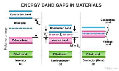
The band gap is the energy difference between the
valence-band maximum and the
conduction-band minimum of a semiconductor. Band-gap
energy is normally expressed in electron volts (eV).
Electrons in the valence band can be excited into available states in
the conduction band when they receive sufficient energy. This process
leaves behind holes in the valence band, producing electron-hole pairs
that can contribute to electrical conduction.
Band gap is therefore an energy property of the semiconductor's
electronic band structure. It is not the name for the movement
of electrons or holes through the material.
In general, a smaller band gap produces a higher intrinsic carrier
concentration at a given temperature, while a larger band gap produces
a lower intrinsic carrier concentration. However, the conductivity of
an actual semiconductor also depends strongly on doping, carrier
mobility, temperature, defects, and material quality.
Learn more about
band-gap energy in semiconductor materials
.
How Do Electrons and Holes Conduct Current?
In an intrinsic semiconductor, thermal or optical excitation can promote
electrons from the valence band into the conduction band, creating
electron-hole pairs.
When an electric field is applied, conduction-band electrons drift in
the direction opposite to the electric field, while
holes behave as positive charge carriers and drift
in the direction of the electric field. Both types of
carriers therefore contribute to electrical current.
The availability and concentration of charge carriers depend on factors
including doping, temperature, illumination, defects, and the
semiconductor's band structure.
In an intrinsic semiconductor, the equilibrium electron
and hole concentrations are equal. In a doped, or
extrinsic semiconductor, one carrier type generally
becomes the majority carrier.
Intrinsic vs. Extrinsic Semiconductors
Intrinsic Semiconductors
An intrinsic semiconductor is an ideally pure or sufficiently
uncompensated semiconductor in which electrical behavior is governed
primarily by thermally generated electron-hole pairs rather than
intentionally introduced dopants.
In thermal equilibrium, intrinsic material has equal electron and hole
concentrations:
n = p = ni
Extrinsic Semiconductors
An extrinsic semiconductor is a semiconductor whose electrical
properties have been intentionally modified through
doping. Adding donor or acceptor impurities changes the
concentration of free charge carriers.
Extrinsic does not mean that the semiconductor is
something other than silicon. Silicon itself can be intrinsic,
n-type, or p-type depending on its impurity and dopant concentrations.
N-Type Semiconductor
N-type silicon is commonly produced by introducing
donor dopants such as phosphorus, arsenic, or antimony.
These dopants provide additional electrons, making electrons the
majority carriers.
P-Type Semiconductor
P-type silicon is commonly produced using an
acceptor dopant such as boron. Boron has three valence
electrons and can accept an electron in the silicon lattice, increasing
the hole concentration. Holes are therefore the majority carriers in
ordinary p-type silicon.
Once silicon is intentionally doped to become n-type or p-type, it is
classified as an extrinsic semiconductor, not an
intrinsic semiconductor.
How Is Silicon Used to Fabricate Semiconductor Devices?
Semiconductor fabrication involves a sequence of highly controlled
processes used to create microscopic electronic structures on and
within a wafer. The exact sequence varies considerably depending on
whether the final device is a CMOS integrated circuit, MEMS sensor,
photodiode, power device, solar cell, or another semiconductor device.
Common fabrication processes include:
-
Wafer Preparation:
Silicon wafers are grown, sliced, shaped, lapped or ground as
required, chemically treated, polished, and cleaned to produce the
required substrate surface.
-
Thermal Oxidation:
When required, silicon can be thermally oxidized to form a controlled
layer of silicon dioxide (SiO2). Thermal oxide can serve
as an electrical insulator, surface passivation layer, masking layer,
or part of a device structure.
-
Photolithography:
A photosensitive resist is deposited and selectively exposed using
a mask or other lithographic system. Development creates a patterned
resist that defines areas for subsequent processing.
-
Etching:
Wet or dry etching can selectively remove exposed material to form
patterned structures in semiconductor, dielectric, or metal layers.
-
Doping:
Dopants can be introduced by processes such as ion implantation,
diffusion, or during epitaxial growth. Donor and acceptor dopants
create controlled n-type and p-type regions.
-
Thin-Film Deposition:
Conductors, dielectrics, semiconductors, and other films can be
deposited using techniques such as chemical vapor deposition (CVD),
physical vapor deposition (PVD), atomic layer deposition (ALD),
epitaxy, and related methods.
-
Annealing and Thermal Processing:
Thermal treatments may be used to activate implanted dopants,
repair crystal damage, modify interfaces, densify films, or drive
diffusion. The purpose of an anneal depends on the fabrication step.
-
Planarization:
Advanced semiconductor fabrication often uses chemical-mechanical
polishing (CMP) to reduce surface topography and prepare the wafer
for additional device layers.
-
Metallization and Interconnects:
Conductive layers are patterned to form electrical contacts and
interconnections between device components.
Many of these processes are repeated to build complex multilayer
structures. After wafer fabrication, individual dies can be electrically
tested, separated by dicing, and packaged to form usable semiconductor
devices.
Common Semiconductor Wafer Applications
Semiconductor wafers provide the starting substrates for a broad range
of technologies, including:
- Microprocessors and memory devices
- Integrated circuits and CMOS devices
- Power transistors and power diodes
- MEMS and microsensors
- Photodiodes and photodetectors
- LEDs and semiconductor lasers
- Solar and photovoltaic cells
- RF and microwave electronics
- Photonic integrated circuits
- Radiation and particle detectors
- Biosensors and lab-on-chip devices
- University semiconductor research
What Is a Semiconductor Wafer?
A semiconductor wafer is a thin substrate made from a
semiconductor material and used as the foundation for fabricating electronic,
photonic, sensing, MEMS, and power devices. Silicon is the most widely used
semiconductor wafer material, but many applications use compound or
wide-band-gap semiconductors.
During semiconductor fabrication, structures are formed on or within the wafer
using processes such as photolithography, etching, thin-film deposition,
oxidation, epitaxy, ion implantation, diffusion, annealing, and
chemical-mechanical polishing (CMP). The exact sequence depends on the
device being manufactured.
A semiconductor wafer is not itself an integrated circuit.
Instead, many individual devices or integrated-circuit dies can be fabricated
across a wafer. After processing and testing, the wafer may be diced into
individual dies for packaging.
Common Semiconductor Wafer Materials
Silicon (Si)
is the dominant substrate for conventional integrated circuits because of its
mature manufacturing infrastructure, useful electrical properties, and ability
to form a high-quality native silicon dioxide (SiO2).
Other important semiconductor materials and substrate platforms include:
-
Gallium Arsenide (GaAs)
– used in RF, microwave, optoelectronic, laser, LED, and photovoltaic
applications.
-
Silicon Germanium (SiGe)
– used in high-frequency electronics and semiconductor heterostructures.
-
Indium Phosphide (InP)
– important for photonic integrated circuits, optical communications,
photodetectors, lasers, HEMTs, and HBTs.
-
Silicon Carbide (SiC)
– a wide-band-gap semiconductor widely used for high-voltage,
high-power, and high-temperature electronics.
-
Gallium Nitride (GaN)
– a wide-band-gap semiconductor used for power electronics,
RF devices, LEDs, and optoelectronics.
-
Zinc Oxide (ZnO)
– a wide-band-gap semiconductor investigated for optoelectronics,
sensors, transparent electronics, and related research.
-
Diamond
– a very-wide-band-gap semiconductor with exceptional thermal
conductivity and potential applications in high-power and
high-temperature electronics.
Sapphire (Al2O3) is also widely
used in semiconductor manufacturing, particularly as a substrate for
epitaxial growth of materials such as GaN. However, sapphire itself is
an electrical insulator rather than a conventional semiconductor.
What Is a Semiconductor in Simple Terms?
A semiconductor is a material whose electrical behavior
can be controlled much more readily than that of a typical metal or
electrical insulator.
Semiconductor conductivity can be modified through
doping, temperature, illumination, electric fields, material
composition, and device structure. This controllability is what
makes semiconductors useful for electronic and photonic devices.
Semiconductors are materials; diodes and transistors are
devices made using semiconductor materials. A semiconductor
should therefore not be defined as a device that simply allows current
to flow in one direction.
Semiconductor materials may be elemental, such as silicon and germanium,
or compounds, such as GaAs, InP, GaN, and SiC.
How Are Silicon Semiconductor Wafers Made?
Semiconductor-grade silicon begins with highly purified silicon feedstock.
Single-crystal silicon ingots are commonly grown using either the
Czochralski (CZ) or
Float-Zone (FZ)
process.
The ingot is then processed into wafers through steps that can include:
- Ingot cropping and diameter shaping
- Wafer slicing
- Edge profiling
- Lapping or grinding
- Chemical etching
- Polishing
- Cleaning
- Inspection and metrology
Device fabrication takes place after the substrate wafer has been prepared.
Depending on the device, fabrication may then involve:
- Photolithography
- Ion implantation or diffusion
- Thin-film deposition
- Etching
- Thermal oxidation
- Annealing
- Metallization
- CMP and planarization
These processes can be repeated many times to construct transistors,
interconnects, dielectric layers, sensors, or other structures across
the wafer.
Common Silicon Wafer Diameters
Silicon wafers are manufactured in multiple diameters. Common research
and industrial sizes include 25.4 mm (1 inch), 50.8 mm (2 inch),
76.2 mm (3 inch), 100 mm, 125 mm, 150 mm, 200 mm, and 300 mm.
300 mm (12 inch) silicon wafers
are widely used in advanced high-volume semiconductor manufacturing.
Smaller diameters remain important for research, legacy fabrication
lines, MEMS, sensors, power devices, and specialized applications.
Wafer thickness is not determined by diameter alone. Standard thicknesses
are used for handling and processing, while wafers can also be thinned
substantially for specialized devices after fabrication.
How Does Temperature Affect a Semiconductor?
Temperature affects several semiconductor properties simultaneously,
including carrier concentration, carrier mobility, band-gap
energy, resistivity, leakage current, and device performance.
In an intrinsic semiconductor, increasing temperature
provides more thermal energy for exciting electrons from the valence
band into the conduction band. Each excitation creates a conduction-band
electron and a corresponding hole in the valence band.
As a result, the intrinsic carrier concentration increases
strongly with temperature. This generally causes the electrical
conductivity of intrinsic semiconductor material to increase as
temperature rises.
Carrier mobility often moves in the opposite direction. At sufficiently
high temperatures, increased lattice vibrations produce stronger
phonon scattering, which generally reduces electron and hole mobility.
Semiconductor conductivity can be written approximately as:
σ = q(nμn + pμp)
where q is the elementary charge,
n and p are the electron and hole
concentrations, and μn and μp are their respective
mobilities.
Therefore, it is not scientifically correct to say simply that increasing
temperature always increases or always decreases semiconductor conductivity.
The result depends on the semiconductor, doping level, temperature range,
carrier concentration, and carrier mobility.
Temperature Regions in Doped Semiconductors
A doped semiconductor can exhibit different temperature regimes:
-
Freeze-out region:
At sufficiently low temperatures, not all dopant atoms are ionized,
so the free-carrier concentration can be relatively low.
-
Extrinsic region:
Over an intermediate temperature range, most dopants are ionized and
the carrier concentration is controlled primarily by the doping level.
-
Intrinsic region:
At sufficiently high temperatures, thermally generated electron-hole
pairs become comparable to or exceed the dopant-generated carrier
concentration.
The temperatures at which these regimes occur depend on the material,
dopant species, dopant concentration, and semiconductor band structure.
What Is an Extrinsic Semiconductor?
An extrinsic semiconductor is a semiconductor whose
electrical properties have been intentionally modified by introducing
dopant atoms.
Extrinsic does not mean that the material is something
other than silicon. Silicon itself becomes extrinsic silicon when
intentionally doped with donor or acceptor impurities.
What Is Semiconductor Doping?
Doping is the controlled introduction of electrically
active impurities into a semiconductor to modify its carrier concentration
and electrical properties.
N-Type Silicon
In silicon, group-V elements such as phosphorus, arsenic, and
antimony can act as donor dopants. They introduce donor states
close to the conduction-band edge and can provide electrons to the
conduction band.
Electrons are therefore the majority carriers in
ordinary
n-type silicon
.
P-Type Silicon
Group-III elements such as boron can act as acceptor
dopants in silicon. Boron has three valence electrons, not five.
Substitutional boron introduces an acceptor state and can increase the
concentration of holes.
Holes are therefore the majority carriers in ordinary
p-type silicon.
Doping does not simply replace the semiconductor's fundamental band gap
with a new “dopant band gap.” Donor and acceptor impurities introduce
energy states associated with the dopants, while the semiconductor retains
its underlying valence and conduction bands. At very high doping
concentrations, additional effects such as band-gap narrowing and
degeneracy may occur.
Electrical Neutrality in Doped Semiconductors
A semiconductor can contain large concentrations of electrons, holes,
and ionized dopants while remaining approximately
electrically neutral overall.
In n-type material, ionized donor atoms carry positive charge after
donating electrons. In p-type material, ionized acceptors carry negative
charge after accepting electrons. Charge neutrality relates the
concentrations of electrons, holes, ionized donors, and ionized acceptors.
N-type material is not automatically more conductive than p-type material.
Conductivity depends on both carrier concentration and carrier
mobility:
σ = q(nμn + pμp)
What Is an Intrinsic Semiconductor?
An intrinsic semiconductor is an ideally pure or
sufficiently uncompensated semiconductor in which the equilibrium carrier
concentrations are determined primarily by thermal generation rather than
intentional doping.
At thermal equilibrium:
n = p = ni
where ni is the intrinsic carrier concentration.
An intrinsic semiconductor does not suddenly “become a semiconductor”
only after it is heated. It is already a semiconductor; temperature
changes the number of thermally generated carriers and therefore its
electrical behavior.
Conduction in an Intrinsic Semiconductor
Thermal energy can excite electrons from the valence band into the
conduction band, leaving holes in the valence band.
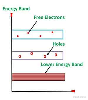
When an electric field is applied, electrons and holes drift in
opposite directions. Electrons, which carry negative charge,
drift opposite to the electric field. Holes behave as positive charge
carriers and drift in the direction of the electric field. Both carrier
motions contribute to conventional electrical current.
This carrier motion is not called a band gap.
The band gap is the energy difference between the
valence-band maximum and the conduction-band minimum.
What Is Band-Gap Energy?
The
band-gap energy
Eg is the energy difference between the
valence-band maximum and the
conduction-band minimum.
It represents the fundamental energy separation relevant to exciting
electrons from valence-band states into conduction-band states.
Band gaps can be characterized using several techniques depending on
the material. Common approaches include optical absorption,
reflectance, photoluminescence, spectroscopic ellipsometry, and
temperature-dependent electrical measurements.
Atomic force microscopy (AFM) is primarily a surface-topography
and force-measurement technique and should not be described as the
standard method for measuring semiconductor band-gap energy.
How Does Band Gap Affect Intrinsic Carrier Concentration?
The intrinsic carrier concentration depends strongly on band-gap energy
and temperature. A commonly used relationship has the form:
ni =
√(NCNV)
exp(−Eg/2kBT)
where NC and NV are the effective densities of
states, Eg is the band gap, kB is Boltzmann's
constant, and T is absolute temperature.
This relationship helps explain why, all else being equal,
a smaller band gap generally produces a higher intrinsic carrier
concentration at a given temperature.
Actual wafer conductivity cannot be predicted from band gap alone,
however. Doping, carrier mobility, temperature, defects, compensation,
and material quality must also be considered.
How Do Holes Move in a Semiconductor?
A hole represents an unoccupied electronic state in the valence band
that can behave as a positive charge carrier.
Hole transport does not mean that a physical positively charged particle
is moving from atom to atom. Instead, neighboring valence electrons can
successively occupy available states, making the vacancy appear to move
through the crystal.
Under an applied electric field, holes drift in the direction of the
field while electrons drift in the opposite direction.
How Do Semiconductors Absorb Light?
Semiconductor optical absorption depends on photon energy and the
material's electronic band structure.
When a photon has sufficient energy for an allowed interband transition,
it can be absorbed and excite an electron from the valence band into the
conduction band, producing an electron-hole pair.
For a simple direct-band-gap semiconductor, strong interband absorption
begins near the band-gap energy. In an
indirect-band-gap semiconductor such as silicon,
momentum conservation means that phonons participate in near-edge
optical transitions.
Photons with energy substantially greater than the band gap can initially
create carriers with excess energy. These carriers typically relax toward
the band edges through interactions with the lattice, converting much of
that excess energy into phonons (heat).
The generated electron-hole pairs can then be separated and collected
in devices such as
solar cells and photodetectors, or they may recombine
radiatively or nonradiatively depending on the semiconductor and device
structure.
Semiconductor Wafers for Different Applications
No single semiconductor material is optimal for every application.
Material selection depends on properties such as band gap, band-gap type,
carrier mobility, breakdown field, thermal conductivity, lattice constant,
optical properties, substrate quality, and fabrication requirements.
-
Silicon:
integrated circuits, MEMS, sensors, photovoltaics, and many power devices.
-
GaAs:
RF electronics, optoelectronics, lasers, LEDs, and high-efficiency
photovoltaic research.
-
InP:
optical communications, photonic integrated circuits, lasers,
photodetectors, HEMTs, and HBTs.
-
SiC:
high-voltage, high-power, and high-temperature electronics.
-
GaN:
power electronics, RF electronics, LEDs, and optoelectronics.
Related Semiconductor Resources
