
I’m interested in purchasing some Sapphire Wafers that are similar to the c-plane sapphire wafers ID 1251 listed in your web site.
The question I have is, are these Double Side Polished wafers optically clear and how much reflectivity is
there? I need to use them to cover LED’s during testing and cannot afford to have an extremely reflective surface that can skew the data.
The info below is from your web page and are the wafers I’m looking at. If you can send me more info
on this product, I can have the engineering team look at it and determine if they are the correct ones for
this project.
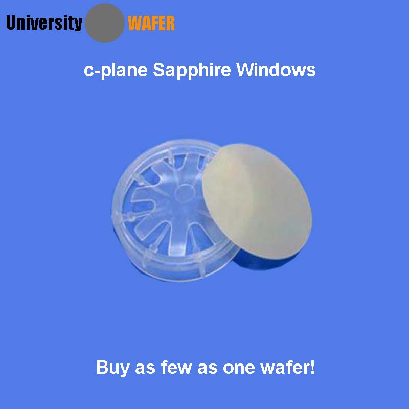
Need C-Plane Sapphire (Al₂O₃) Substrates?
High-quality single-crystal sapphire wafers in C-plane <0001>, A-plane, R-plane orientations — polished to your spec. Sizes from 2″ to 150 mm, ready to ship.
- DSP or SSP surface finish
- Tight orientation tolerance for epitaxy
- Custom cuts & thicknesses available
- Used for GaN, AlN, LED, RF, and optical applications
Trusted by universities, research labs, and industry worldwide.
C-Plane Sapphire Wafers Used as LED Cover
A chief technology officer requested a quote for the following:
Reference #226444 for specs and pricing.
Get Your C-Plane Sapphire Wafer Quote FAST! Or, Buy Onlineand Start Researching Today!
Why Use C-Plane Sapphire?
The high anisotropy of c-plane sapphire makes it more resistant to scratches than asymmetrical sapphire. It is stable enough to withstand the pressure and heat, making it a better material for laser-cutting and microelectronics applications. In addition, the crystalline structure of c-plane sapphire is more pronounced than that of asymmetrical sapphire.
In addition to optical properties, sapphire is highly abrasive and has a higher resistance than silicon. This property makes it ideal for SOI devices. The increased resistance, low parasitic capacitance, and improved film carrier mobility make c-plane sapphire a desirable choice for many industrial and scientific applications. Its transparency means it is suitable for a variety of products.
The properties of c-plane sapphire also make it an excellent choice for a wide range of crystalline structures. Because it is so hard, a single-crystalline crystal of this material has high electrical insulation. Its facets are highly polished to make them more useful for a variety of applications. Moreover, it has a broad optical transmission range. The main advantage of c-plane sapphire is that it has a low dielectric loss.
C-plane sapphire wafers are not as common as other specifications. However, the fabricated flakes of c-plane sapphire are very hard and have a high hardness, which makes them an excellent choice for semiconductor manufacturing. Because of these characteristics, c-plane sapphire is also highly conductive, allowing it to be used as a semiconductor material.
The c-plane sapphire wader is a superior choice for microelectronics and laser-cutting applications. Its lower resistance and reduced parasitic capacitance make it the ideal material for SOI devices. Because of its properties, sapphire can be used in a wide range of applications, including photovoltaics, lasers, and semiconductors.
C-plane sapphire wafers are available in all Oris and can be used in many different applications. They are widely used in a variety of semiconductor devices, including high-frequency transistors and microelectronics. There is also no limit to their use in a wide range of industries. Its low resistance, low thermal conductivity, and high transparency make it a desirable material for SOI technology.
Because of its high anisotropy, c-plane sapphires are more scratch-resistant and are better suited for laser-cutting. They also resist heat and pressure, making them an excellent choice for many applications. In fact, a wide range of semiconductor applications are now possible thanks to the availability of c-plane sapphire in standard and custom packaging.
Because sapphires are so transparent and have a relatively high resistance, they are highly suitable for various electrochemical and electronic devices. Despite its high resistance, C-plane sapphire has a high level of transielectrical properties that make it an ideal material for SOI devices. In addition, it reduces parasitic capacitance and improves film carrier mobility. Furthermore, it is highly transparent, making it an excellent choice for many applications.
C-plane sapphire has a remarkably uniform band-gap distribution, making it a useful substrate for various optical applications. It is the least expensive of the three types of sapphire and is commonly used in high-precision optical applications. It has a high surface hardness, and has low transmission and reflected wavefront distortion. It is also used in the production of HB-LED and is highly resistant to thermal shock.
C-plane sapphire is an excellent material for microelectromechanical devices. Its high resistance makes it an ideal substrate for microelectromechanical devices. Additionally, sapphire offers a low iep, which is the most important quality for a semiconductor device. In turn, this makes sapphire an attractive material for high-precision optical components.
What Does C-M plane 0.2 deg on Sapphire Mean?
It is still the C-palne Al2O3,C-M plane 0.2 deg means " C-Plane(0001) Mis-cut 0.2deg towards M-axis "
It can be tough to source c-plane sapphire because not all suppliers carry this product. And if you do find a supplier, it's likely that their stock is limited and they won't be able to meet your needs in a timely manner.
C-Plane Sapphire from UniversityWafer, Inc. is the answer. We are your one-stop shop for c-plane sapphire products of all shapes and sizes. We have a large inventory of c-plane sapphire that is always in stock and ready to ship.
What Sapphire Substrate Diameters are Available?
We have a large selection of stadard diameters and custom dimension availble. Please send us your specs or click below:
What is a C-Plane Sapphire Wafer and what is its application?
A C-plane sapphire wafer is a thin, flat disc made from sapphire crystal with a c-plane  Ori. The c-plane is a specific crystallographic Ori of sapphire that has a hexagonal structure, and the wafer is called c-plane because it is cut perpendicular to the c-axis.
Sapphire wafers are used in a wide range of applications, particularly in the semiconductor industry. C-plane sapphire wafers are particularly useful in the production of light-emitting diodes (LEDs), as they offer a number of desirable properties, including high transparency in the visible and near-infrared regions, excellent thermal conductivity, and high chemical and mechanical durability.
In addition to LEDs, c-plane sapphire wafers are also used in the manufacture of power electronic devices, such as diodes and transistors, as well as in the production of high-temperature and high-pressure sensors, watch faces, and other precision optics.
Sapphire is a popular choice for high-precision optical instruments. The atomic-scale properties of sapphire allow for highly accurate measurements.
C-Plane Sapphire Wafer Inventory
Below are just a sample of our inventory. Click here to buy online.
| ID | Diam | Orientation | Thick (µm) | Polish | Description |
|---|---|---|---|---|---|
| 3156 | Rectangle | <0001> | 500 | SSP | |
| Sapphire wafer — C ±0.5° • 2.5 mm × 25 mm × 0.5 mm • Single-side polished | |||||
| 3467 | 10 mm × 10 mm | <0001> | 430 | DSP | |
| C-plane, ±0.3° • POOR SURFACE QUALITY • NON-REFUNDABLE • Sold “As-Is”. | |||||
| 3409 | 6.0 mm | <0001> | 100 | DSP | |
| Please contact us for more information. | |||||
| 1251 | 50.8 mm | <0001> | 430 | DSP | |
| C-M plane 0.2°. | |||||
| 1306 | 50.8 mm | <0001> | 430 | SSP | |
| C to M-plane by 0.2 ± 0.1° off. | |||||
| 2768 | 50.8 mm | <0001> | 330 | DSP | |
| C-plane <0001> off M-plane <1-100> 0.2 ± 0.1° | |||||
| 3407 | 50.8 mm | <0001> | 100 | DSP | |
| C-plane off to M-plane by 0.2° | |||||
| 1732 | 100 mm | <0001> | 650 | SSP | |
| Orientation: C-plane off 0.2 ± 0.1° to M-plane (leftwards from primary). 0 ± 0.1° off to A-plane. Surface: 1× epi-polished (Ra < 0.2 nm); 1× fine-ground (Ra 0.6–1 µm). Primary flat length 30 ± 1 mm; Primary flat orientation A-plane ±0.3°. TTV ≤ 20 µm; Bow −15 to 0 µm. | |||||
| 2562 | 100 mm | <0001> | 650 | DSP | |
| C-M plane 0.2° • Double-side polished • Ra < 0.35 nm • Primary flat 32.5 ± 2.5 mm • Warp < 21 µm • TTV < 16 µm. | |||||
| 3444 | 100 mm | <0001> | 500 | DSP | |
| 3460 | 150 mm | <0001> | 950 | DSP | |
| SEMI standard notch • Other specs unknown • Sold “As-Is”. | |||||
What is A-Plane Sapphire?
 A-plane sapphire is a high-quality material with high purity. The material is incredibly durable, making it an ideal choice for semiconductor applications. In addition, sapphire is more affordable than asymmetrical sapphire, making it an excellent material for thin-film technology. Compared to other types of materials, c-plane sapphire is also more brittle, which means that it is more prone to breakage.
In a previous experiment, researchers studied the electrical evaluation of c-plane sapphire wafers. These studies demonstrated that the majority carrier lifetime is a factor of four, which is lower than the corresponding value in silicon. In contrast, the minority carrier lifetime is about one ns3, making c-plane sapphire an excellent material for SOI devices.
Several advantages of c-plane sapphire over Si include its higher resistance. In microelectronic devices, sapphire provides better performance, reduced parasitic capacitance, and improved film carrier mobility. The materials are also highly transparent, making them suitable substrates for a wide range of applications. If the high-resistance properties of silicon aren't enough for your application, sapphire is an excellent choice for these technologies.
The material properties of c-plane sapphire are identical to those of other sapphire components. They are Mohs 9 in hardness and can be fabricated in as little as 0.4 mm. They have a transmitted wave front error of less than l/10 nm at 632.8 nm. Unlike quartz, the optical properties of c-plane sapphirite are very stable.
The study was conducted using a C-plane patterned sapphire substrate. Its full-width at half-max of c-plane sapphire was 732 nm. Its radiation hardness was found to be 612.2 nm. This makes it an ideal choice for epitaxial growth of III-V and II-VI compounds. This research demonstrates the versatility of a sapphire chip.
The c-plane sapphire is a common material used in semiconductors. The structure of c-plane sapphire is determined by its band-gap distribution. HF, SC1, and SC1 are used to treat the sapphire. The phosphate buffer layer makes it a useful material for various applications. These treatments can be used to smooth the surface of a sapphire crystal.
C-plane sapphire is also known as zero-degree sapphire or c-plane sapphire. It is the cheapest of the three types and is commonly used for high-precision optical applications. Its chemical resistance is exemplary, and its surface hardness is second only to diamond. In addition to its optical properties, a C-plane sapphire is known for its low-transmittedtransmitted wavefront distortion.
A variety of different types of sapphire are available in nature. The deep blue sapphire is a deep blue stone that contains iron and titanium. The crystalline structure of a sapphire depends on many physical properties, including temperature. A C-plane sapphire is best for applications that require optical quality. These materials are abrasive, but they are also tough and resistant to wear.
The c-plane sapphire has a high degree of anisotropy. This means that it is more resistant to scratches. The c-plane sapphire is a superior choice for laser-cutting applications. Moreover, it is highly stable, as it can withstand heat and pressure. So, if you are looking for a new type of cut to your specifications, it is well worth considering the c-plane sapphire.
A C-plane sapphire is a transparent, monocrystalline sapphire glass. It has a low density, and its high-density patterned counterparts are transparent. The c-plane is also a superior choice for microelectronics. A n-plane n-planer is an example of a n-plane n-planing.
We have a large selection of c-plane sapphire with both thick and thin wafers single and double side polished.
What are C-plane Sapphire Wafer Applications?
One of the most important characteristics of c-plane sapphire is its high optical transmittance. Its optical properties make it a perfect material for ultraviolet and near-infrared applications. C-plane sapphier are also stronger than standard glass substrates. C-plane sapphire is also resistant to high-temperature, thermal shock on the surface and scratch resistant.
C-plane sapphire wafers are transparent or opaque depending on if it's single or double side polished. It's amorphous, which means that it is transparent to light. C-plane Al2O3 is an optimal choice for microelectronics and hybrid modules. Its TDs are a key feature in high-precision photonics.
C-plane sapphire wafers are great for Infrared (IR) applications and sapphire are often used as a base wafer for growing III-V and II-VI compounds including Gallium Arsenide, and Gallium Nitride to fabricate blue LED and laser diodes.
Which Sapphire Plane is Easiest to Cleave?
A researcher requested the following:
Question:
We are planning to buy sapphire wafers and I have a few questions: - we need to cleave the wafer in squared chips. Which crystallographic Ori is better suited for this? I saw you have different possibilities. - would it be possible to buy only one or two, or the order includes a fixed number of wafers?
Answer:
Crystallographic Ori C-plane is best for cleave, to buy only one or two is ok.