Wafers for Photoconductive Antenna Fabrication
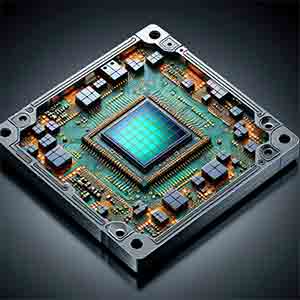
UniversityWafer supplies photoconductive antenna substrates for terahertz generation, THz detection, ultrafast optoelectronics, infrared sensing, and photodetector research. Common materials include low-temperature-grown GaAs, semi-insulating GaAs, InGaAs, InP, ZnTe, InSb, and selected silicon substrates.
Researchers can request wafers with custom orientation, thickness, diameter, resistivity, doping, surface finish, epitaxial structure, and quantity.
Research Request: Photoconductive Antenna for 1550 nm Excitation
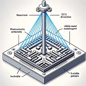
A PhD student requested assistance selecting a semiconductor wafer for fabricating a photoconductive antenna excited by a femtosecond fiber laser operating at a wavelength of 1550 nm.
The researcher requested information about:
- Available semiconductor wafer materials and specifications
- Recommended substrates for 1550 nm photoconductive antenna operation
- Pricing and research-quantity availability
- Lead times and delivery options
- Custom specifications and possible alternatives
Substrate selection for 1550 nm excitation often differs from conventional 800 nm photoconductive antenna systems. InGaAs-based materials are frequently considered because their bandgap is compatible with near-infrared optical excitation.
Reference #278559 for specifications and pricing.
Get Your Photoconductive Antenna Wafer Quote FAST!
Or,
Buy Online
and Start Researching Today!
What Substrates Are Used for Photoconductive Antennas?
Photoconductive antennas (PCAs) are widely used in
terahertz spectroscopy and imaging
.
They convert ultrafast optical pulses into THz electromagnetic radiation or detect incoming THz signals by generating a short-lived photocurrent in a semiconductor material.
An effective photoconductive antenna substrate typically requires suitable optical absorption, short carrier lifetime, high carrier mobility, high breakdown strength, and compatibility with metal electrode fabrication.
Low-Temperature-Grown GaAs
Low-temperature-grown gallium arsenide (LTG GaAs) is one of the most widely used materials for photoconductive antennas excited near 800 nm. Growth at reduced temperature introduces crystal defects that act as rapid carrier-recombination centers, enabling short electrical pulses and broad THz bandwidth.
Semi-Insulating GaAs
Semi-insulating GaAs
provides high electrical resistivity and low dark current. It is used in photoconductive switches, THz emitters, detectors, RF devices, and optoelectronic research, although its carrier lifetime may be longer than that of LTG GaAs.
InGaAs for 1550 nm Photoconductive Antennas
Indium Gallium Arsenide (InGaAs)
is an important material for photoconductive antennas driven by 1550 nm fiber lasers. Its narrower bandgap allows efficient absorption of near-infrared light that standard GaAs does not absorb effectively.
Fe-doped InGaAs, ion-implanted InGaAs, low-temperature-grown InGaAs, and InGaAs/InAlAs heterostructures may be used to reduce carrier lifetime and improve THz emission or detection performance.
A PhD student requested an InGaAs wafer for photodetector research.
Reference #248354 for specifications and pricing.
Indium Phosphide
Indium Phosphide (InP)
may serve as a substrate for InGaAs-based epitaxial structures and advanced near-infrared photoconductive devices. It offers good lattice compatibility with selected InGaAs compositions.
InGaAs/InAlAs Heterostructures
InGaAs/InAlAs heterostructures can be engineered for high carrier mobility, electrical confinement, and compatibility with 1550 nm excitation. These multilayer structures are used in advanced THz photoconductive emitters, receivers, and high-speed optoelectronic devices.
Zinc Telluride
Zinc Telluride (ZnTe)
is commonly used for optical rectification and electro-optic sampling rather than as a conventional biased photoconductive antenna substrate. Its nonlinear optical properties make it valuable in THz generation and detection systems.
Indium Antimonide
Indium Antimonide (InSb)
has high electron mobility and a narrow bandgap, making it useful in infrared detectors, magnetoresistive devices, and selected terahertz research applications.
Silicon
Silicon wafers
are not as common as GaAs or InGaAs for conventional photoconductive antennas, but they may be used as mechanical support substrates, high-resistivity platforms, photonic integration substrates, or components in hybrid THz devices.
How to Choose a Photoconductive Antenna Substrate
The correct substrate depends strongly on the optical pump wavelength and intended THz application.
-
Near 800 nm: LTG GaAs and related GaAs materials are commonly considered.
-
Near 1550 nm: InGaAs-based materials are generally more suitable because they absorb telecom-wavelength light.
-
Low dark current: High-resistivity or semi-insulating materials are preferred.
-
Broad THz bandwidth: Short carrier lifetime and fast recombination are important.
-
High output power: Carrier mobility, breakdown field, electrode spacing, thermal handling, and optical absorption must all be considered.
Photoconductive Antenna Electrode Materials
Photoconductive antenna fabrication also requires patterned metal electrodes. Common choices include gold, titanium, chromium, aluminum, and multilayer adhesion/contact stacks.
Electrode geometry, gap size, antenna shape, metal thickness, surface quality, and substrate resistivity can significantly affect THz efficiency, bandwidth, dark current, and device reliability.
Information to Include in Your Wafer Request
- Optical pump wavelength, such as 800 nm or 1550 nm
- THz emitter, detector, switch, or photodetector application
- Preferred substrate or epitaxial material
- Wafer diameter and thickness
- Crystal orientation
- Carrier lifetime or mobility requirements
- Resistivity or semi-insulating specification
- Surface finish and epitaxial-ready requirements
- Required quantity
What Are Photodetector Devices?
Photodetector devices detect visible light, ultraviolet radiation,
infrared radiation, or other portions of the electromagnetic spectrum and convert
the absorbed energy into an electrical signal.
Depending on the detector design, the output may appear as an electrical current,
voltage, resistance change, or temperature-dependent response. Photodetectors are
widely used in optical communications, infrared sensing, medical imaging,
astronomy, industrial automation, scientific instrumentation, digital cameras,
environmental monitoring, and consumer electronics.
Photodiodes
Photodiodes are semiconductor devices that convert absorbed
photons into electron-hole pairs. Many photodiodes operate under reverse bias,
allowing the generated charge carriers to produce a measurable photocurrent.
Photodiodes are commonly used in fiber-optic communications, light meters,
scientific instruments, solar-energy research, medical equipment, and visible
or infrared sensing systems.
Phototransistors
Phototransistors operate similarly to photodiodes but provide
internal current amplification. When light reaches the photosensitive region,
it controls the current flowing between the collector and emitter.
These devices are used in optical switches, object detectors, encoders,
optoisolators, counting systems, alarms, and light-sensitive control circuits.
Photomultiplier Tubes
Photomultiplier tubes (PMTs) are highly sensitive light
detectors capable of measuring extremely weak optical signals. When a photon
strikes the photocathode, it releases an electron that is amplified through a
sequence of dynodes.
PMTs are used in spectroscopy, fluorescence measurements, medical imaging,
particle detection, astronomy, nuclear instrumentation, and other low-light
applications.
Avalanche Photodiodes
Avalanche photodiodes (APDs) operate under a high reverse-bias
voltage near the breakdown region. The strong internal electric field accelerates
photogenerated charge carriers and produces additional carriers through impact
ionization.
This internal gain improves detector sensitivity, making APDs useful for
fiber-optic communications, LiDAR, laser range finding, fluorescence detection,
time-of-flight measurements, and low-light sensing.
Charge-Coupled Devices
Charge-coupled devices (CCDs) are image sensors formed from
arrays of light-sensitive pixels. Each pixel stores electrical charge in
proportion to the amount of incident light.
The accumulated charge is transferred across the sensor to an output amplifier.
CCDs are commonly used in scientific cameras, astronomy, microscopy,
spectroscopy, medical imaging, and high-quality digital imaging.
Complementary Metal-Oxide-Semiconductor (CMOS) image sensors
use arrays of photosensitive pixels, with each pixel generally containing
charge-to-voltage conversion circuitry.
CMOS sensors can integrate amplifiers, noise correction, timing circuits, and
digital processing directly onto the chip. They are widely used in smartphones,
cameras, automobiles, medical instruments, machine-vision systems, and
surveillance equipment.
Photoresistors and Light-Dependent Resistors
Photoresistors, also called
light-dependent resistors (LDRs), change electrical resistance
according to the intensity of incident light. Their resistance generally
decreases as light intensity increases.
LDRs are commonly used in automatic lighting systems, alarms, brightness
controls, photographic light meters, toys, and ambient-light sensing circuits.
Pyroelectric Detectors
Pyroelectric detectors respond to temperature changes caused
by absorbed infrared radiation. The change in temperature alters the
polarization of the pyroelectric material and produces an electrical signal.
These detectors are used in infrared motion sensors, gas analysis, flame
detection, spectroscopy, thermal sensing, security systems, and non-contact
temperature measurement.
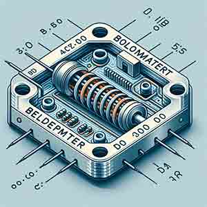
Bolometers
Bolometers measure incident electromagnetic radiation by
detecting the heating of an absorbing material. As the absorber temperature
changes, its electrical resistance or another measurable property also changes.
Bolometers are especially useful for infrared, far-infrared, millimeter-wave,
and terahertz detection. Applications include thermal imaging, astronomy,
spectroscopy, security systems, environmental monitoring, and scientific
instrumentation.
Quantum Dot Photodetectors
Quantum dot photodetectors use semiconductor nanocrystals to
absorb light and generate charge carriers. Their spectral response can be
adjusted by changing the quantum-dot material, composition, shape, and particle
size.
These devices are being researched for infrared imaging, multispectral
detection, flexible electronics, low-cost photodetection, biomedical sensing,
and integration with silicon-based electronics.
Photodetector Applications
Photodetectors support telecommunications, medical imaging, astronomy, industrial
automation, environmental sensing, defense systems, consumer electronics,
spectroscopy, automotive sensing, and scientific research.
Selecting the correct detector requires consideration of the target wavelength,
sensitivity, response time, noise level, quantum efficiency, active area, operating
temperature, amplification requirements, and fabrication method.
Are (111) Substrates Suitable for Photodetector Fabrication?
A (111) crystal orientation may be useful for selected
photodetector structures, but it should not be chosen only because it is assumed to
provide better carrier mobility. Detector performance also depends on semiconductor
composition, epitaxial quality, surface recombination, interface defects, contact
design, doping, and fabrication conditions.
Silicon (100) is widely selected for conventional semiconductor processing because
of its compatibility with oxidation, lithography, and established device
fabrication techniques. Silicon (111) may be preferred for selected epitaxial
growth, anisotropic etching, surface-science, nanostructure, and specialized
optoelectronic applications.
Substrates Used to Fabricate Infrared Photodetectors
Infrared photodetectors may be fabricated using
silicon, germanium, InGaAs, InP, GaAs, InSb, HgCdTe, GaN, SiC,
and other semiconductor materials. The correct substrate depends on the target
wavelength range, detector temperature, required sensitivity, response speed, and
compatibility with the necessary epitaxial layers.
Silicon is commonly used for visible and near-infrared detection, while germanium
and InGaAs extend sensitivity farther into the near-infrared spectrum. InSb and
HgCdTe are frequently investigated for longer-wave infrared detection.
A Ph.D. researcher requested assistance with the following project:
We are working on infrared photodetectors and
optoelectronic devices
.
What substrate can you recommend?
Reference #ONLQ43013 for specifications and pricing.
Related Photodetector Resources
Explore related semiconductor substrates, infrared detector materials,
photoconductive devices, and optoelectronic fabrication resources.