
We are developing a fabrication process for near-infrared photodetectors integrated with conventional electronic devices. Do you offer germanium deposited on silicon wafers, or can you fabricate Ge-on-Si substrates for research?
Substrates for Near-Infrared Photodetectors
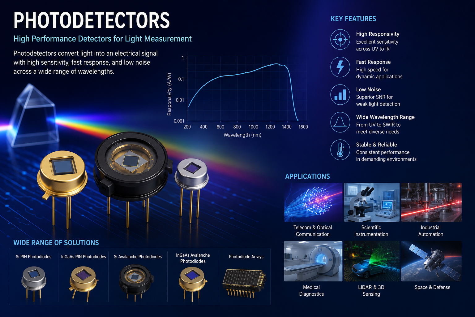
UniversityWafer supplies silicon, germanium, Ge-on-Si, GaN, AlGaN, SiC, and intrinsic silicon wafers for photodetectors operating in the visible, ultraviolet, and near-infrared (NIR) spectrum. Our substrates are used in photodiodes, photodetector arrays, CMOS image sensors, optical sensors, satellite imaging systems, photonic integrated circuits (PICs), and optoelectronic research requiring high responsivity, low dark current, and excellent detectivity.
An electrical engineering researcher requested:
Reference #93774 for specifications and pricing.
Get Your Photodetector Wafer Quote FAST! Or, Buy Online and start your research today.
Position-Sensitive Detectors for Space Applications
A customer developing a four-quadrant position-sensitive detector (PSD) for satellite sun sensing requested substrates capable of operating from 200–1100 nm with low dark current, low capacitance, fast response time, and reliable performance in low Earth orbit. The application also required high external quantum efficiency (EQE), stable spectral response, and excellent detectivity across the visible and near-infrared spectrum.
- 25 × 25 mm die size
- 20 × 20 mm active area
- Operating wavelength: 200–1100 nm
- Dark current < 3 nA
- Capacitance < 3000 pF
- Operating temperature: -40°C to 75°C
Reference #94426 for pricing.
GaN, AlGaN & SiC Photodetector Wafers
Wide bandgap materials such as GaN, AlGaN, and SiC are commonly selected for UV photodetectors because of their low leakage current, excellent radiation resistance, high breakdown voltage, and outstanding detectivity. These materials are widely used for flame detection, aerospace systems, environmental monitoring, and other harsh-environment optoelectronic applications.
A MEMS researcher requested single-crystal GaN or AlGaN wafers for fabricating blue and UV photodetectors and semiconductor diodes with low leakage current.
Reference #115249 for specifications and pricing.
Black Silicon for High-Efficiency Photodetectors
Black silicon features nanoscale surface structures that dramatically reduce reflection and increase optical absorption across the visible and near-infrared spectrum. The enhanced light trapping improves responsivity, quantum efficiency, and overall photodetector sensitivity while maintaining low reflection losses.
- Higher optical absorption
- Improved photodetector sensitivity
- Higher responsivity and quantum efficiency
- Reduced surface reflection
- Visible, NIR, and terahertz applications
- Image sensors and photovoltaic devices
Undoped Silicon for PIN Photodetector Arrays
Researchers developing PIN photodiode arrays frequently request high-resistivity float-zone silicon because of its low defect density, long carrier lifetime, high carrier mobility, and excellent electrical performance. These properties contribute to lower noise equivalent power (NEP), improved detectivity, and better device performance in weak-light photodetectors.
We are looking for 3-inch, double-side polished, intrinsic float-zone silicon wafers with resistivity greater than 8,000 Ω·cm for PIN photodetector arrays.
UniversityWafer Recommended:
- 3" SEMI Prime silicon wafer
- 525 ±25 µm thickness
- Float-zone intrinsic silicon
- <100> orientation ±0.5°
- >8,000 Ω·cm resistivity
- Double-side polished (DSP)
Reference #131421 for pricing and availability.
What Substrates Are Used in Photodetectors?
Photodetectors convert light into electrical signals and are used in optical communications, imaging systems, spectroscopy, biomedical instruments, autonomous vehicles, satellite sensors, industrial automation, optical sensors, machine vision, and scientific research. The choice of substrate directly affects spectral response, responsivity, detectivity, dark current, quantum efficiency (QE), external quantum efficiency (EQE), response time, and operating wavelength.
Common photodetector substrates include silicon, germanium (Ge), GaAs, GaN, SiC, and silicon-on-insulator (SOI). Each material is selected based on the wavelength range, optical absorption, carrier transport properties, and overall device performance required.
Silicon Photodetectors
Silicon is the most widely used substrate for photodetectors operating in the visible and near-infrared spectrum. Silicon photodiodes offer low noise, fast response times, excellent uniformity, high responsivity, and compatibility with standard CMOS fabrication processes. Silicon also provides excellent carrier lifetime and carrier mobility, making it ideal for high-performance photodetectors and CMOS image sensors.
Researchers frequently use high-resistivity float-zone silicon, intrinsic silicon, double-side polished wafers, and SOI substrates to fabricate photodiodes, phototransistors, avalanche photodiodes (APDs), position-sensitive detectors (PSDs), and high-speed optical sensors. Device performance is commonly evaluated using parameters such as detectivity, noise equivalent power (NEP), spectral response, and external quantum efficiency.
Germanium-on-Silicon (Ge-on-Si) Photodetectors
Germanium deposited on silicon extends the detection wavelength beyond conventional silicon devices into the near-infrared region. Ge-on-Si photodetectors are widely used in fiber-optic communications, LiDAR, optical interconnects, silicon photonics, and photonic integrated circuits (PICs) because germanium efficiently absorbs wavelengths around 1.3 μm and 1.55 μm.
Combining germanium with silicon enables CMOS-compatible manufacturing while producing highly sensitive weak-light photodetectors with excellent responsivity and low noise for optical communication systems, machine vision, imaging, and integrated photonic devices.
Wide Bandgap Photodetectors
Wide bandgap semiconductors such as GaN, AlGaN, and SiC are commonly used for UV photodetectors. Their high breakdown voltage, low leakage current, excellent radiation resistance, and high detectivity make them suitable for aerospace, flame sensing, environmental monitoring, space exploration, and harsh-environment electronics.
GaN and SiC photodetectors are also widely investigated for solar-blind UV detection because of their fast response times, low dark current, outstanding thermal stability, and excellent long-term reliability.
Transparent Conductive Electrodes
Many photodetectors incorporate transparent conductive films to maximize light transmission while maintaining excellent electrical conductivity. Common transparent electrode materials include Indium Tin Oxide (ITO), graphene, transparent conductive oxides, and dielectric-metal-dielectric (DMD) multilayers.
These coatings improve optical transmission and quantum efficiency while supporting applications in flexible electronics, CMOS image sensors, display technologies, photonic devices, and high-efficiency optoelectronic systems.
Ohmic and Schottky Contacts
Electrical contacts play a critical role in photodetector performance. Ohmic contacts minimize contact resistance and improve carrier collection, while Schottky contacts are commonly used in high-speed photodetectors and ultraviolet photodetectors where low capacitance, fast switching, and high detectivity are required.
The choice of contact metal depends on the semiconductor material and desired electrical characteristics, with gold, titanium, nickel, aluminum, platinum, and germanium alloys commonly used in device fabrication.
Black Silicon for High-Sensitivity Photodetectors
Black silicon features a nanostructured surface that dramatically reduces reflection and increases optical absorption across the visible and near-infrared spectrum. The enhanced light trapping significantly improves responsivity, quantum efficiency, and photodetector sensitivity while reducing optical losses.
Black silicon is increasingly used for image sensors, biosensors, terahertz devices, optical sensing, and high-efficiency photodiodes requiring broadband spectral response.
Photodetector Arrays
Photodetector arrays consist of multiple photodiodes fabricated on a single semiconductor substrate. They are widely used in spectrometers, machine vision, satellite imaging, medical diagnostics, optical communications, LiDAR, facial recognition systems, industrial inspection, and position-sensitive detectors. Silicon remains the preferred material for visible-light arrays, while germanium and III-V compound semiconductors extend detector performance into longer infrared wavelengths.
Custom Photodetector Substrates
UniversityWafer supplies silicon, germanium, SOI, GaN, AlGaN, SiC, and custom semiconductor substrates for photodetector research. Available options include float-zone silicon, intrinsic silicon, double-side polished wafers, epitaxial wafers, oxide-coated wafers, and custom substrate specifications for UV, visible, near-infrared, avalanche photodiode (APD), CMOS image sensor, and photonic integrated circuit development.