Why is the Orientation of Silicon Important?
Silicon Orientation is a vital part of the process of producing carbon nanotube (CNT) based electrode and conductor materials. It is a key prerequisite in many of the applications and technologies we use every day.
Buy Your Silicon Wafers Online and Save!
With the ability to produce and deliver better performing devices, more efficient thermal insulation, and greener, safer building materials, the use of silicon-wafer edge engineering is becoming very important. But what exactly is it and how does it work?
Get Your Quote FAST! Or, Buy Online and Start Researching Today!
Silicon Crystalline Orientation Applications
In principle, the orientation of crystalline materials determines their optical, electrical, and mechanical properties. It's not that simple though. Alloys, like glass and silver, are made of multiple layers of powdered materials which are bonded together with other metallic oxides. There are also several different types of crystalline structures including amorphous, planar, and amoeboid. Each has its own peculiarities, which may affect their mechanical, optical, and chemical properties.
Silicon wafer-crystalline substrates are prepared from a variety of materials including aluminum, tin, steel, copper, and nickel alloys. Their composition is primarily dependent on the function they will play. Some of them are heat treated, some are solid friction free, and some are liquid conductors. In addition, the thickness, shape, and location of the crystalline substrates in the wafer can affect their use in electronics and optoelectronics applications. Here are some examples:
Silicon Wafer Orientation in Optoelectronic Research: In electronics and optoelectronics research, the silicon orientation of the substrates has a profound effect. As research has proven, using a particular crystalline structure greatly influences the conductivity, optical, and thermal properties of the final product. Some of these effects are called substrate interactions which are due to chemical reactions between certain substrates. In some instances, substrate interactions are purely a function of temperature. Yet, most of these effects are the result of substrate design mistakes or lack of knowledge regarding how to properly align them.
Silicon Crystal Etching Processes: For applications where crystal alignment is important, but also important to maintain the correct crystal symmetry, engineers rely upon computer simulation techniques. This enables the simulation of various crystal structures using different conformers, substrates, and the various equipment used during the crystal etching process. Silicon simulations provide a great deal of insight into the efficiency of the fabrication process.
Silicon Wafer Design & Production: Another application of silicon wafer inspection comes into play when wafer production requires specific, even machined marks. To ensure consistent quality in products, engineers must know which marks will work for which types of substrates. These mark positions can be validated against a large database of potential wafer structures and compositions. Through this method, accurate, real-time feedback can be obtained on a substrate layout that was produced using one particular software package. This provides engineers with the ability to quickly identify areas of concern during the wafer process as well as provide direction for overall manufacturing production.
Non- Silicon Alloys: A very interesting application of silicon wafer orientations is their impact on heat dissipation. Non- Silicon alloys are usually marked with a black stripe across their surface. While they are effective at preventing heat conduction through their flat surfaces, this coating also prevents heat from penetrating the surface of the component. Instead, this heat energy is redirected to the interior of the component. These components have become very popular in applications requiring extreme temperatures, such as rocket-engine parts.
Membrane Technology: Membranes offer unique advantages over traditional methods of substrate attachment. They can form a protective layer between an injection mold's parting line and the work piece. This makes them a wonderful choice for high-volume, high-tech etching processes. Because these Membrane products can withstand a high amount of heat, their cost-effective operations make them a logical choice when it comes to Membrane substrate design and operation. Many companies offer a wide range of different membrane technologies, and there is likely a technology that will best suit your unique manufacturing needs.
Crystal And Single Crystal Orientation: Single crystals and multi-crystals are growing in popularity for numerous reasons. The most-common of these reasons centers around their ability to create a sharp, clean edge on most surfaces. However, other benefits include their ability to emit negative ions, which increase workability and enhance product quality. Single crystal and multi-crystal processing offer many benefits for component fabrication. For example, this processing method is ideal for making extremely thin wafers and thicker layers.
Silicon Orientation: A wafer's surface can be one of three different orientations. These three common silicon wafer surface orientations include: perpendicular, horizontal, and vertical. Although the physical description for each of these surface states that they are "perpendicular" in nature, each of these silicon wafer substrate orientations has applications in different situations. For example, the most commonly used substrate orientations result in a sharp, clean edge, while others may produce an "articulated" or "wavy" edge. Depending upon your manufacturing process needs, this may be a determining factor when selecting the correct silicon wafer substrate.
As mentioned earlier, many of the most popular substrate orientations are considered "perpendicular" in nature. Examples of this silicon wafer orientation include: flat, diamond, planar, and Membrane. A flat substrate is considered flat because it maintains its width, thickness, and face-flatness throughout the function and/or process. For example, a rectangular wafer blade cut with a diamond-silicon wafer can be expected to maintain the same face-flatness throughout its length. In addition, flat substrates provide superior cut-to-cut-contact times between products.
Another common silicon wafer substrate orientation is diamond-to-crystal. As the name would suggest, diamond-to-crystal wafers are made by cutting a sheet of silicon wafer into regular diamond shapes. This provides a clean, smooth surface that can be polished like other flat substrates. As this diamond-to-crystal wafer cut does not use "perpendicular" symmetry, the resulting products have somewhat irregular edges. This makes diamond-to-crystal wafers particularly useful for cutting delicate surfaces, such as thin-metal laminates.
The third common substrate used in the manufacture of chips and etching is a "planar" wafer. Planar wafers are manufactured using cross-section designs and in some cases with internal cavity. The internal cavity serves as an etching medium, which is commonly made from anodized aluminum or copper. A planar wafer is preferred over other materials for etching because of its high etching performance and can also withstand heat up to 400 degrees Celsius, which makes it ideal for applications requiring extremely high temperatures.
Please help me to know what is difference between 001, 010, 100 for crystal orientation.
The different Miller indices you see, such as (001), (010), and (100), represent various crystallographic orientations of the crystal surface. Here's a breakdown of what each one typically represents in the context of silicon dioxide (SiO2) crystals:
-
(001) orientation: This indicates that the surface of the crystal is perpendicular to the [001] direction, which is typically aligned along the "c-axis" in a crystal lattice. This orientation can affect properties such as surface reactivity, chemical etching behavior, and electronic properties.
-
(010) orientation: This means the crystal's surface is perpendicular to the [010] direction, aligned with the "b-axis." Similar to (001), this orientation impacts the material's mechanical, thermal, and optical properties, as well as how it interacts with different processes like deposition or etching.
-
(100) orientation: The surface here is perpendicular to the [100] direction, often aligned with the "a-axis." This is a common orientation used for various types of epitaxial growth and has distinct properties in terms of symmetry, etching, and bonding characteristics.
In general, different crystal orientations will influence factors like:
- Anisotropy: The variation of properties in different directions.
- Thermal expansion: Different crystal orientations may expand or contract differently with temperature changes.
- Chemical reactivity: Certain surfaces may etch faster or slower depending on their orientation.
- Deposition quality: Thin films or coatings may adhere differently depending on the crystal's orientation.
The choice of orientation often depends on the specific application, such as in microfabrication, optical systems, or surface treatments. Let me know if you need further clarification on these aspects!
Reference #317316 for specs and pricing.
Silicon Wafer Flat Edge Crystal Orientation
A PhD student requested help with the following questions.
Question:
I have a question regarding silicon wafers. I’ve noticed that one edge of the wafer is flat rather than perfectly circular, which I understand is related to indicating the crystal orientation. Could you please clarify which direction the flat edge corresponds to when the wafer has a (100) crystal orientation.
I just wanted to know about the direction of silicon (100) like the flat edge should face which direction that it shows certain crystal map. I sent a picture to make it clear what I mean. I appreciate if you can let me know about this
Answer:
You're absolutely right that the flat edge on a silicon wafer is used to indicate the crystal orientation and sometimes the type and doping of the wafer.
Given your wafer spec:
-
Diameter: 50.8 mm (2-inch)
-
Orientation: ⟨100⟩
-
Type: P-type / B (Boron-doped)
-
Resistivity: 0.001–0.005 Ω·cm
-
Thickness: 280 µm
-
Polish: SSP (Single Side Polished)
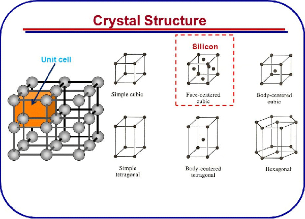
Silicon Crystal Structure
As emerging technologies like photonics, quantum computing, and advanced sensor arrays rely more on engineered materials, scientists look to classical semiconductors like silicon for inspiration. Understanding silicon’s crystal structure can guide the development of new materials and structures with tailored properties.
Common Silicon Crystal Structure Applications
1. Semiconductor Devices and Integrated Circuits:
The diamond cubic crystal structure of silicon is the foundational template for nearly all modern integrated circuits (ICs). From microprocessors and memory chips to signal processors and logic gates, the precise arrangement of silicon atoms enables consistent electrical properties and stable doping profiles. This stability and uniformity form the backbone of the global electronics industry.
2. Solar Cells:
Crystalline silicon—both monocrystalline and polycrystalline—remains the most widely used material for photovoltaic (PV) solar cells. Its well-understood crystal structure contributes to reliable electron transport and efficient photon absorption, yielding the high energy conversion efficiencies that make silicon-based solar panels the industry standard.
3. Microelectromechanical Systems (MEMS):
Silicon’s crystalline structure imparts mechanical strength and chemical stability, which are key traits in MEMS devices such as accelerometers, gyroscopes, pressure sensors, and microfluidic components. The regular crystalline lattice allows for precise etching and micromachining, enabling the creation of tiny, intricate mechanical elements on silicon wafers.
4. Sensors and Detectors:
Silicon’s predictable crystal lattice ensures that its electronic properties, such as carrier mobility and band structure, are highly reproducible. This makes it ideal for a range of sensors—image sensors in digital cameras and smartphones, photodiodes for optical communication systems, and radiation detectors in medical imaging systems—where stable performance and reliable calibration are crucial.
5. Silicon Photonics:
Although silicon is an indirect bandgap semiconductor (which makes it less efficient as a light emitter), its crystal structure and compatibility with CMOS processes have driven the field of silicon photonics. Silicon waveguides, modulators, and photodetectors leverage the uniform and well-controlled crystal lattice to integrate optical components into silicon chips, aiming for reduced cost and enhanced performance in data communication and signal processing.
In all these applications, the crystalline structure of silicon provides a consistent, reliable framework that enables precise control over its electrical, mechanical, and optical properties, laying the groundwork for countless innovations in electronics and renewable energy technologies.
Why is Having The Crrect Silicon Crystal Structure Important?
1. Electronic Properties and Device Performance:
Silicon’s diamond cubic crystal structure ensures a uniform and well-defined arrangement of atoms. The resulting periodicity and lattice symmetry are essential for predictable band structures and carrier transport properties. If the crystal structure is distorted or has too many defects, the mobility of electrons and holes can decrease, impairing the performance and efficiency of devices like transistors, integrated circuits, and solar cells.
2. Doping Consistency and Control:
Doping—introducing controlled amounts of impurity atoms—relies on a stable and defect-free crystalline framework. A properly formed silicon lattice allows dopant atoms to occupy well-defined lattice sites, resulting in consistent electrical characteristics across the wafer. In contrast, irregularities or defects can lead to clustering, unintended doping variations, and non-uniform electrical behavior, making device fabrication more difficult and less reliable.
3. Mechanical Stability and Process Reliability:
A correct crystal structure enhances the mechanical strength and durability of silicon wafers. Manufacturing techniques such as photolithography, etching, and wafer thinning all depend on a stable crystalline foundation. Poor crystal quality can cause issues like wafer breakage, uneven thinning, or compromised MEMS structures, negatively impacting production yields and device longevity.
4. Reduced Defects and Improved Yield:
Lattice defects like dislocations, vacancies, and interstitials can degrade device performance or cause functional failures. Ensuring that silicon grows with the proper crystal structure reduces these defects, leading to higher production yields, better reliability, and longer device lifetimes. This is critical for high-volume semiconductor manufacturing, where even minor defect rates can translate into significant cost and quality issues.
5. Consistent Optical and Thermal Properties:
Advanced devices, especially those in silicon photonics or high-power electronics, rely on predictable optical and thermal characteristics. Proper silicon crystallinity ensures stable refractive indices, predictable absorption spectra, and effective thermal conduction. These factors are vital for achieving reliable, high-performance components in data communications, sensing, and power conversion applications.
In essence, having the correct silicon crystal structure underpins nearly every stage of semiconductor fabrication and device operation. It guarantees uniform and predictable material properties, enabling the precision and performance that define modern electronics and photonics.
What is Silicon Wafer Crystal Orientation?
Typically, single crystals are ordered with the desired orientation. Usually, these orientations are determined by the application. The orientation of a single crystal is specified when ordering it. Orientation can be "none required" or "random". It should be indicated by its Miller or Bravais index and tolerance. Listed below are some of the most common uses for single crystals. In addition to their use in optical devices, single crystals are also used in various applications, such as semiconductors and photonics.
In most cases, the crystals grow from a parent substance, which can be solid, liquid, or gas. If the growth of a single crystal is done from an ion, the parent substance is a solid. In the case of liquids, the growth can take place in a gas or liquid. The orientation of the single crystal can influence the outcome of an experiment. Fortunately, there are numerous ways to determine the orientation of a single crystal.
UniversityWafer, Inc. sells all orientations including silicon 100, 111, 110, 112, 211, 511 etc. Please let us know your wafer specification and quantity for an immediate quote.
What is the difference between (100), (110) and (111) Silicon Wafers?
100, 110, and 111 are crystallographic planes or directions in a crystal lattice of a silicon wafer. These planes and directions are identified by their Miller indices, which are a set of three integers that define the orientation of the planes or directions relative to the crystal lattice.
In a silicon wafer, the (100) plane is a crystal plane that is perpendicular to the <100> direction, which is a line parallel to the y-axis of the crystal lattice. The (110) plane is a crystal plane that is perpendicular to the <110> direction, which is a line at a 45-degree angle to the x- and y-axes of the crystal lattice. The (111) plane is a crystal plane that is perpendicular to the (111) direction, which is a line at a 54.7-degree angle to the x-, y-, and z-axes of the crystal lattice.
The orientation of the planes and directions in a silicon wafer can affect the electrical and mechanical properties of the wafer and the devices that are fabricated on it. For example, the (111) plane is typically preferred for high-quality epitaxial growth, while the (100) plane is preferred for photolithography and device processing. The choice of plane or direction may also depend on the specific application or process requirements.
What is the difference between 100 110 and 111 silicon wafers?
100, 110, and 111 are crystallographic planes or directions in a crystal lattice of a silicon wafer. These planes and directions are identified by their Miller indices, which are a set of three integers that define the orientation of the planes or directions relative to the crystal lattice.
In a silicon wafer, the (100) plane is a crystal plane that is perpendicular to the <100> direction, which is a line parallel to the y-axis of the crystal lattice. The (110) plane is a crystal plane that is perpendicular to the <110> direction, which is a line at a 45-degree angle to the x- and y-axes of the crystal lattice. The (111) plane is a crystal plane that is perpendicular to the <111> direction, which is a line at a 54.7-degree angle to the x-, y-, and z-axes of the crystal lattice.
The orientation of the planes and directions in a silicon wafer can affect the electrical and mechanical properties of the wafer and the devices that are fabricated on it. For example, the (111) plane is typically preferred for high-quality epitaxial growth, while the (100) plane is preferred for photolithography and device processing. The choice of plane or direction may also depend on the specific application or process requirements.
What Silicon Orientation Do I Need?
Orientation needs depends on what your using the silicon wafers for. If your cleaving wafers then a (111) orientation will be more difficult to work with while (100) will cleave just fine.
Cleaving Silicon Wafers
Cleavingis a process used to break or split a silicon wafer into smaller pieces or chips. There are several methods for cleaving silicon wafers, including mechanical cleaving, laser cleaving, and chemical cleaving.
Mechanical cleaving involves using a sharp blade or diamond scribe to score or mark the surface of the wafer along a desired cleave plane. The wafer is then bent or twisted to create a crack at the scored line, and the wafer is broken or split along this line.
Laser cleaving involves using a focused laser beam to create a precise, controlled crack in the wafer. This method allows for very precise cleaving and is often used for high-value or high-precision applications.
Chemical cleaving involves using a chemical solution or etchant to etch a line or groove in the wafer along the desired cleave plane. The wafer is then mechanically bent or twisted to create a crack at the etched line, and the wafer is split along this line.
Regardless of the method used, it is important to ensure that the cleave is clean and smooth to minimize defects and damage to the wafer. Cleaving is typically done in a controlled environment, such as a cleanroom, to minimize contamination.
If you lack the proper spec sheet then a use this simple test to find your silicon wafer's orientation.

Take a nail and press against the center of your silicon wafer. Then take a hammer and hit the head of the nail. If the wafer breaks into 4 pieces then the orientation is (100). If the wafer shatters into many different sized pieces then the orientation is (111).
Lecture on Orientation of Single Crystal
Miller Indices - Difference Between Silicon Wafer <100> & <111>
Classify silicon wafer orientation and include (100), (111), (110), (211), (511).

(100) (010) and (001) are exactly the same and all can be called (100) orientation!
Silicon wafer flats are used to determine the silicon wafer's orientation as in the image below.

Notice that the silicon wafers in the image above have their edges cut out at different areas. These cut-out edges are called flats. The location of the flats is how you determin the crystal orientation of the silicon wafer.
What Silicon Orientation Should I Use for Laser Micromachining?
Clients often ask us which wafer orientation spec would work for their research.
A research client purchased one wafer of each orientation to see which orientation would work best for laser surface engineering for laser micromachining research.
Silicon Wafer Items Used:
Si Item #783 (100)
Si Item #2358 (110)
Si Item #3351 (111)
Researching laser micro-material processing using ultra-short laser pulses, from process development, to process management, to control systems and more.
Can X-Rady Diffrection Determine Cystal Orienation?
X-ray diffraction is an optical technique used to determine a crystal's orientation. It is a fast, accurate, and precise method for determining the orientation of a single crystal. It provides information that relates the crystal's position to the orientation of a material template. This process allows researchers to refine the structure with higher precision and predict future properties. It also allows scientists to make more advanced designs, which are often only possible with single crystals.
What Silicon Orientation Do I Need?
Orientation needs depends on what your using the silicon wafers for. If your cleaving wafers then a (111) orientation will be more difficult to work with while (100) will cleave just fine.
Cleaving Silicon Wafers
Cleaving is a process used to break or split a silicon wafer into smaller pieces or chips. There are several methods for cleaving silicon wafers, including mechanical cleaving, laser cleaving, and chemical cleaving.
Mechanical cleaving involves using a sharp blade or diamond scribe to score or mark the surface of the wafer along a desired cleave plane. The wafer is then bent or twisted to create a crack at the scored line, and the wafer is broken or split along this line.
Laser cleaving involves using a focused laser beam to create a precise, controlled crack in the wafer. This method allows for very precise cleaving and is often used for high-value or high-precision applications.
Chemical cleaving involves using a chemical solution or etchant to etch a line or groove in the wafer along the desired cleave plane. The wafer is then mechanically bent or twisted to create a crack at the etched line, and the wafer is split along this line.
Regardless of the method used, it is important to ensure that the cleave is clean and smooth to minimize defects and damage to the wafer. Cleaving is typically done in a controlled environment, such as a cleanroom, to minimize contamination.
If you lack the proper spec sheet then a use this simple test to find your silicon wafer's orientation.
Take a nail and press against the center of your silicon wafer. Then take a hammer and hit the head of the nail. If the wafer breaks into 4 pieces then the orientation is (100). If the wafer shatters into many different sized pieces then the orientation is (111).
Lecture on Orientation of Single Crystal
Miller Indices - Difference Between Silicon Wafer <100> & <111>
Classify silicon wafer orientation and include (100), (111), (110), (211), (511).
(100) (010) and (001) are exactly the same and all can be called (100) orientation!
Silicon wafer flats are used to determine the silicon wafer's orientation as in the image below.
Notice that the silicon wafers in the image above have their edges cut out at different areas. These cut-out edges are called flats. The location of the flats is how you determin the crystal orientation of the silicon wafer.
What Silicon Orientation Should I Use for Laser Micromachining?
Clients often ask us which wafer orientation spec would work for their research.
A research client purchased one wafer of each orientation to see which orientation would work best for laser surface engineering for laser micromachining research.
Silicon Wafer Items Used:
Si Item #783 (100)
Si Item #2358 (110)
Si Item #3351 (111)
Researching laser micro-material processing using ultra-short laser pulses, from process development, to process management, to control systems and more.
Can X-Rady Diffrection Determine Cystal Orienation?
X-ray diffraction is an optical technique used to determine a crystal's orientation. It is a fast, accurate, and precise method for determining the orientation of a single crystal. It provides information that relates the crystal's position to the orientation of a material template. This process allows researchers to refine the structure with higher precision and predict future properties. It also allows scientists to make more advanced designs, which are often only possible with single crystals.
What are 111 Oriented Silicon Wafers?
Among the three common orientations, 111 is the most common. It is the most common type and is the most widely used in the semiconductor industry. It is easier to cleve and has the lowest cost, but there are other factors that should be considered when selecting the orientation. Here are some examples of 111-oriented silicon wafers. Let us examine each one of these options in more detail. 1.1 Orientation
Orientation: During fabrication, Si111 wafers are usually etched in 110- or 100-oriented directions. This 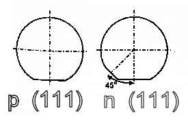 etching method is preferred as it results in less distortion during fabrication. The etching process is also faster on the 111-oriented planes than on the 110-oriented planes. The slowest etching rate of all the wet anisotropic etchants is achieved on the Si111 planes.
Orientation: When a silicon wafer is oriented in 111- or 110-degree orientation, the atoms are at a 90-degree angle to the primary flat. The result is that the etching speed is faster on the 114- or 111-oriented silicon wafers. However, a downside of 111-oriented silicon is that it is more difficult to fabricate complex structures using the polarization of the atoms.
Orientation: 111- and 114-oriented silicon wafers have different properties than the traditional 109-plane. Typically, the 111-oriented silicon wafer has less lateral undercutting. This makes it difficult to control the microstructure. Alternatively, a VSI manufacturer will provide a primary flat and a 115- or 118-oriented silicon wafer.
(643) Orientation for Epitaxial Electrodeposition Research
University Scientist:
"We are interested in the Si <643> wafer which I read from this paper (https://pubs.acs.org/doi/pdf/10.1021/jacs.8b09108). I am wondering if this is something you can produce and if so, what is an approximate price per 4" piece."
UniversityWafer, Inc. Quoted:
Item
HS69 Qty 5
Silicon wafers, per SEMI Prime, P/P 4" (100.0±0.5mm)Ø×525±25µm,
p-type Si:B [643]±0.5°, Ro=(10-20)Ohmcm,
TTV<10µm, Bow<20µm, Warp<30µm,
Both-sides-polished, NO Flats,
Sealed in Empak or equivalent cassette.
Reference #266753 for pricing

