
How Silicon's Periodic Table Properties Relate to Semiconductor Wafers
Silicon (Si) has atomic number 14 and belongs to Group 14 of the periodic table. Its four valence electrons allow each silicon atom to form four covalent bonds in a crystalline lattice, creating the highly ordered structure used in single-crystal silicon wafers. This atomic structure is one of the key reasons silicon is so useful for semiconductor devices.
Silicon as a Semiconductor Material
Pure crystalline silicon is an intrinsic semiconductor. At room temperature, it has a band gap of approximately 1.12 eV, allowing its electrical conductivity to be controlled through temperature and, more importantly, through the intentional addition of dopant atoms.
Silicon's electrical behavior can be modified to create p-type silicon or n-type silicon. This ability to engineer carrier concentration is fundamental to semiconductor devices such as diodes, transistors, integrated circuits, sensors, and photovoltaic cells.
How Periodic Table Elements Are Used to Dope Silicon
Dopants are selected partly because of their position on the periodic table. Elements from neighboring groups can introduce either excess electrons or electron deficiencies into the silicon crystal lattice.
- Group 13 elements, particularly boron, are commonly used as acceptor dopants to produce p-type silicon.
- Group 15 elements, such as phosphorus and arsenic, are commonly used as donor dopants to produce n-type silicon.
Dopant concentration can be controlled over a wide range to produce wafers with specific resistivity, conductivity type, and electrical characteristics for research and device fabrication.
Silicon Crystal Orientation
Semiconductor-grade silicon is typically grown as a single crystal using processes such as Czochralski crystal growth or Float Zone processing. The resulting crystal is sliced and polished into wafers with defined crystallographic orientations.
Common orientations include (100), (110), and (111). Crystal orientation affects properties such as surface atomic arrangement, oxidation behavior, carrier mobility, mechanical response, and etching characteristics, making orientation an important wafer specification.
Why Silicon Dioxide Makes Silicon Especially Useful
Another major advantage of silicon is its ability to form a high-quality native oxide, silicon dioxide (SiO2). Thermal silicon dioxide is widely used as an electrical insulator, surface passivation layer, masking material, and dielectric in semiconductor processing.
The combination of controllable semiconductor behavior and a stable oxide has helped silicon become the dominant material for integrated circuits, MEMS, sensors, power devices, photovoltaics, and microfabrication.
Silicon Wafer Specifications for Research
Researchers selecting silicon wafers should consider more than just the element itself. Important substrate specifications include:
- Wafer diameter
- Crystal orientation
- Conductivity type – p-type or n-type
- Resistivity
- Dopant species
- Wafer thickness
- Single-side or double-side polish
- Crystal growth method
These properties influence how the wafer behaves during microfabrication, oxidation, lithography, thin-film deposition, etching, and electrical device fabrication.
Silicon Wafers for Education and Semiconductor Research
UniversityWafer supplies silicon wafers for materials science, semiconductor physics, electrical engineering, nanotechnology, MEMS, photovoltaics, and university laboratory research. Substrates are available with a range of orientations, resistivities, dopant types, thicknesses, and surface finishes.
Get Your Silicon Wafer Quote FAST! Or Buy Silicon Wafers Online and start your research today.
Where Is Silicon on the Periodic Table?
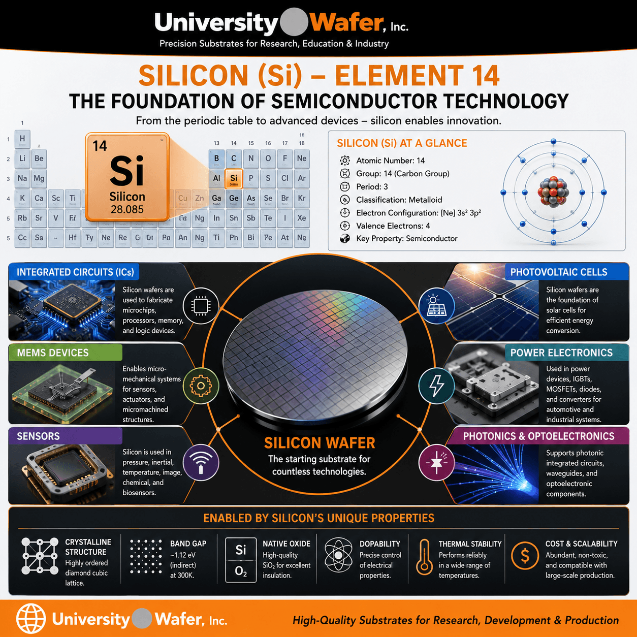
Silicon (Si) is element 14 on the periodic table. It is located in Group 14, also known as the carbon group, and Period 3. Silicon is commonly classified as a metalloid because its physical and electrical behavior falls between that of typical metals and nonmetals.
Silicon has four valence electrons, which allows each atom to form four covalent bonds in the crystalline lattice. This bonding structure is central to the electrical and mechanical behavior of single-crystal silicon wafers used in semiconductor fabrication.
Silicon Periodic Table Properties
| Property | Value |
|---|---|
| Element Name | Silicon |
| Symbol | Si |
| Atomic Number | 14 |
| Group | 14 (Carbon Group) |
| Period | 3 |
| Classification | Metalloid |
| Standard Atomic Weight | 28.085 |
| Electron Configuration | [Ne] 3s² 3p² |
| Valence Electrons | 4 |
| Room-Temperature Band Gap | Approximately 1.12 eV |
Why Silicon Works So Well as a Semiconductor
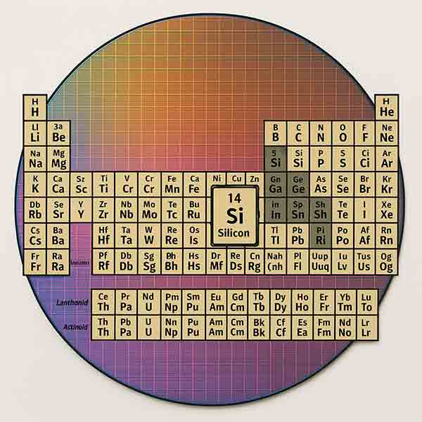
Silicon is useful in electronics because its electrical conductivity can be deliberately modified by introducing controlled amounts of dopant atoms. This makes it possible to create p-type silicon and n-type silicon, the two basic conductivity types used throughout semiconductor device fabrication.
Silicon also forms a high-quality oxide, silicon dioxide (SiO2), which can function as an electrical insulator, masking layer, surface-passivation layer, and dielectric. The ability to combine silicon with a stable oxide has been especially important in the development of modern integrated circuits.
How Dopants Relate to the Periodic Table
The periodic table helps explain why certain elements are effective silicon dopants. Silicon is in Group 14 and has four valence electrons. Elements in neighboring groups can alter the number of available charge carriers when incorporated into the silicon lattice.
- Boron (B) — a Group 13 acceptor dopant commonly used to produce p-type silicon.
- Phosphorus (P) — a Group 15 donor dopant commonly used to produce n-type silicon.
- Arsenic (As) — a Group 15 donor dopant used in n-type silicon for selected device processes.
Dopant concentration influences carrier concentration and wafer resistivity, so researchers often specify both conductivity type and resistivity when ordering silicon substrates. Learn more about silicon wafer doping techniques.
Silicon Compared with Other Semiconductor Materials
Silicon remains the dominant semiconductor platform for many electronic and MEMS applications, but other materials can provide advantages where higher frequency, wider band gap, optical emission, or high-temperature operation is required.
| Material | Key Advantage | Common Applications |
|---|---|---|
| Silicon (Si) | Mature processing, scalable manufacturing, high-quality SiO₂ | Integrated circuits, MEMS, sensors, photovoltaics |
| Gallium Arsenide (GaAs) | High electron mobility and direct band gap | RF devices, microwave electronics, lasers, photodetectors |
| Silicon Carbide (SiC) | Wide band gap and high thermal conductivity | Power electronics, high-temperature devices, EV power systems |
| Gallium Nitride (GaN) | Wide band gap, high breakdown field, high-frequency capability | RF electronics, LEDs, power conversion, communications |
| Germanium (Ge) | High carrier mobility and infrared response | Photonics, infrared detectors, specialized semiconductor devices |
Other Periodic-Table Elements Used in Semiconductor Fabrication
Semiconductor manufacturing relies on many elements in addition to silicon. Their roles depend on their electrical, chemical, optical, and mechanical properties.
- Boron (B) — p-type silicon dopant
- Phosphorus (P) — n-type silicon dopant
- Arsenic (As) — n-type dopant and component of GaAs
- Oxygen (O) — component of SiO2 and other oxides
- Nitrogen (N) — component of GaN, AlGaN, and silicon nitride
- Gallium (Ga) — component of GaAs and GaN
- Indium (In) — component of InP and other III-V compounds
- Aluminum (Al) — metallization and compound-semiconductor alloys
- Copper (Cu) — interconnect metallization in integrated circuits
How the Periodic Table Connects to Wafer Engineering
The periodic table is more than a chemistry reference for semiconductor engineers. It helps explain bonding behavior, valence-electron count, dopant selection, compound-semiconductor composition, oxidation, and material compatibility.
These relationships guide the selection of substrates and processing materials for CMOS, MEMS, sensors, photovoltaics, photonics, RF electronics, and power devices. UniversityWafer supplies a range of semiconductor substrates including silicon wafers, SOI wafers, epitaxial silicon, SiC wafers, and GaAs substrates for research and device development.
Related Silicon and Semiconductor Resources
- What Is Silicon? – Learn about silicon properties, crystal structure, semiconductor behavior, and wafer applications.
- Silicon Wafers – Explore silicon substrates by diameter, orientation, resistivity, dopant type, and surface finish.
- Silicon Wafer Applications – See how silicon wafers are used in electronics, MEMS, sensors, photovoltaics, and research.
- Silicon Wafer Doping Techniques – Compare methods used to introduce dopants and control silicon electrical properties.
- P-Type Silicon – Learn how acceptor dopants such as boron create hole-dominated conductivity.
- N-Type Silicon – Learn how donor dopants such as phosphorus and arsenic create electron-dominated conductivity.
- Silicon Lattice Constant – Explore the crystalline structure and lattice dimensions of silicon.
- Metalloids on the Periodic Table – Learn why silicon is classified as a metalloid and how metalloids differ from metals and nonmetals.
- Thermal Oxide on Silicon – Learn how high-quality SiO2 layers are formed on silicon wafers.
- Silicon-on-Insulator (SOI) Wafers – Explore silicon device layers isolated by a buried oxide layer.
- What Is a Semiconductor Wafer? – Learn how wafers serve as the starting substrates for semiconductor device fabrication.
- Photolithography – Learn how circuit and microdevice patterns are transferred onto semiconductor wafers.