Example Research Requirements:
- Application: Underwater photovoltaic power generation
- Requested band-gap range: 1.8–2.3 eV
- Target output: approximately 12 V
- Panel area: less than 1 m2
- Materials considered: III-V photovoltaic semiconductors
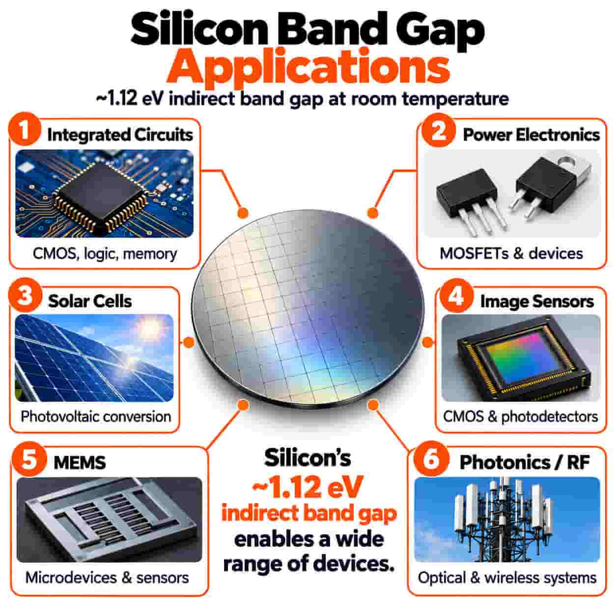
Crystalline silicon has an indirect band gap of approximately 1.12 eV at room temperature (300 K). This energy gap between the valence and conduction bands strongly influences silicon's electrical and optical behavior, making band-gap physics important for understanding integrated circuits, solar cells, photodetectors, sensors, and other semiconductor devices.

Crystalline silicon (Si) has an indirect band gap of approximately 1.12 eV at room temperature (about 300 K). The band gap, Eg, is the energy difference between the valence-band maximum (VBM) and the conduction-band minimum (CBM).
Silicon's band gap is fundamental to its behavior as a semiconductor. Electrons can be excited from the valence band into the conduction band by thermal energy, optical absorption, or other excitation mechanisms. When this occurs, an electron is promoted into an available conduction-band state and a corresponding hole is left in the valence band.
These mobile electrons and holes can contribute to electrical conduction. Their concentrations and transport properties are influenced by temperature, doping, electric fields, crystal quality, and device structure.
Get Your Silicon Wafer Quote FAST! Or, Buy Wafers Online and start researching today!
The commonly quoted room-temperature band gap of crystalline silicon is approximately:
Eg ≈ 1.12 eV at 300 K
This value is not constant with temperature. As the temperature of crystalline silicon increases, its band gap generally decreases. At temperatures approaching 0 K, the band gap is approximately 1.17 eV.
The temperature dependence of the silicon band gap is often represented empirically using the Varshni relation:
Eg(T) = Eg(0) - αT2 / (T + β)
where Eg(0) is the extrapolated band gap at 0 K and α and β are material-specific empirical parameters.
Silicon is classified as an indirect-band-gap semiconductor because its valence-band maximum and conduction-band minimum occur at different values of crystal momentum.
In bulk crystalline silicon, the valence-band maximum occurs at the Γ point, while the conduction-band minima occur along the Δ directions between Γ and X in reciprocal space.
Because these states have different crystal momentum, a near-band-edge optical transition generally requires the participation of a phonon in addition to a photon so that both energy and crystal momentum can be conserved.
This is an important difference between silicon and direct-band-gap semiconductors such as gallium arsenide (GaAs) , where the conduction-band minimum and valence-band maximum occur at the same crystal momentum.
| Property | Indirect Band Gap | Direct Band Gap |
|---|---|---|
| Example | Silicon (Si) | Gallium Arsenide (GaAs) |
| VBM and CBM Momentum | Different crystal momentum | Same crystal momentum |
| Near-Band-Edge Optical Transition | Typically requires phonon participation | Can occur without phonon assistance |
| Radiative Recombination | Relatively inefficient | Relatively efficient |
| Typical Applications | ICs, MOSFETs, solar cells, sensors | LEDs, lasers, photonics, high-speed electronics |
The silicon band structure describes the allowed electron energy states in crystalline silicon as a function of crystal momentum. Understanding this structure helps explain silicon's electrical, optical, and carrier-transport properties.
The valence band contains the highest occupied electronic states at absolute zero in an ideal intrinsic semiconductor. A completely filled band does not produce a net electrical current.
When an electron is excited from the valence band, the missing electron can be described as a hole. Holes behave as mobile positive charge carriers and are particularly important in P-type silicon .
The conduction band contains allowed electronic states above the band gap. Electrons occupying suitable conduction-band states can respond to an applied electric field and contribute to electrical current.
In N-type silicon , donor impurities provide additional electrons, making electrons the majority carriers under typical conditions.
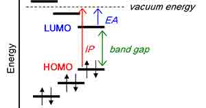
The band gap is an energy range between the valence and conduction bands in which an ideal bulk crystal has no allowed electronic states.
For crystalline silicon at room temperature:
Eg ≈ 1.12 eV
The existence of this finite band gap is one of the properties that distinguishes a semiconductor such as silicon from a conventional metal.
Photon energy and wavelength are related approximately by:
E(eV) ≈ 1240 / λ(nm)
A photon energy equal to silicon's room-temperature band gap of about 1.12 eV corresponds to a wavelength of approximately 1,107 nm (1.11 µm).
However, because silicon has an indirect band gap, optical absorption near the band edge is relatively weak and involves phonon-assisted transitions. It is therefore more accurate to describe approximately 1.1 µm as the near-band-edge wavelength region rather than as a perfectly sharp optical cutoff.
At shorter wavelengths, photons have more than enough energy to generate electron-hole pairs, although absorption depth varies strongly with wavelength.
Silicon's band gap influences many important semiconductor properties, including intrinsic carrier concentration, optical absorption, leakage behavior, temperature dependence, and electron-hole generation.
At a given temperature, band-gap energy is one of the factors controlling intrinsic carrier concentration. In simplified form:
ni ∝ exp[-Eg / (2kT)]
where ni is the intrinsic carrier concentration, Eg is the band gap, k is the Boltzmann constant, and T is absolute temperature.
This means that, all else being comparable, a larger band gap generally produces a lower intrinsic carrier concentration at a given temperature. Electrical conductivity in a real semiconductor, however, also depends strongly on doping concentration, carrier mobility, defects, electric fields, and temperature. Band gap alone does not determine the conductivity of a doped semiconductor.
Silicon's approximately 1.12 eV band gap allows it to absorb a broad portion of the terrestrial solar spectrum, which is one reason crystalline silicon is widely used for photovoltaic devices.
Photons with sufficient energy can generate electron-hole pairs in silicon. Photons with energies below the relevant absorption threshold are not efficiently absorbed through ordinary band-to-band transitions, while photon energy substantially above the band gap ultimately contributes excess energy primarily as heat after carrier thermalization.
The optimum band gap for a photovoltaic device depends on the incident spectrum and device architecture. Tandem and multijunction solar cells use semiconductors with different band gaps so that different portions of the spectrum can be converted more efficiently.
A PhD candidate researching underwater solar-energy harvesting requested photovoltaic materials with band gaps between approximately 1.8 and 2.3 eV. The higher requested band gaps were intended to better match portions of the optical spectrum that can remain available underwater.
Example Research Requirements:
Water does not transmit the terrestrial solar spectrum uniformly. Infrared radiation is strongly attenuated, while portions of the visible spectrum can penetrate farther depending on water depth, clarity, dissolved material, and suspended particles.
A requested band-gap range of 1.8–2.3 eV corresponds approximately to photon wavelengths of 690–540 nm. Higher-band-gap photovoltaic junctions can therefore be of interest when designing devices for an underwater spectrum that is depleted in longer wavelengths.
Conventional GaInP/GaAs/Ge triple-junction photovoltaic cells combine semiconductor junctions with different band gaps. The germanium bottom junction has a relatively small band gap of approximately 0.67 eV and primarily extends the cell's response toward longer wavelengths.
Because longer-wavelength and infrared radiation are strongly attenuated by water, the Ge bottom junction may provide less useful photocurrent in some underwater environments than it does under terrestrial illumination.
Depending on water depth and spectral conditions, a device architecture emphasizing higher-band-gap III-V junctions may provide better spectral matching. The optimum architecture cannot be determined from band gap alone; it depends on the measured underwater spectral irradiance, junction current matching, optical losses, depth, water composition, and device design.
| Semiconductor | Approx. Band Gap at Room Temperature | Band-Gap Type |
|---|---|---|
| Silicon (Si) | ~1.12 eV | Indirect |
| Germanium (Ge) | ~0.66–0.67 eV | Indirect |
| Gallium Arsenide (GaAs) | ~1.42 eV | Direct |
| Indium Phosphide (InP) | ~1.34 eV | Direct |
| Gallium Phosphide (GaP) | ~2.26 eV | Indirect |
| 4H-SiC | ~3.26 eV | Indirect |
Understanding silicon's band gap and electronic band structure is important for designing and analyzing:
UniversityWafer supplies silicon wafers with customizable diameter, crystal orientation, conductivity type, resistivity, thickness, surface finish, and other specifications for semiconductor device and materials research.
The band gap of a semiconductor can be investigated using several experimental techniques. For crystalline silicon, common approaches include optical absorption, photoconductivity, photoluminescence, spectroscopic methods, and temperature-dependent electrical measurements.
Optical absorption is particularly useful because the absorption spectrum contains information about electronic transitions between the valence and conduction bands. However, the analysis must account for the fact that silicon is an indirect-band-gap semiconductor.
Near silicon's fundamental absorption edge, an optical transition generally involves both a photon and a phonon to satisfy energy and crystal-momentum conservation. Consequently, the absorption edge of silicon differs from that of a direct-band-gap semiconductor such as gallium arsenide (GaAs) .
Yes. The band gap of crystalline silicon is temperature dependent. It is approximately 1.17 eV near 0 K and decreases to approximately 1.12 eV at room temperature.
As temperature rises, interactions between electrons and the vibrating crystal lattice, together with thermal expansion, modify the electronic band structure and generally reduce the band-gap energy.
This temperature dependence matters in semiconductor devices because temperature also affects intrinsic carrier concentration, carrier mobility, leakage current, junction behavior, and device performance.
Conventional doping of silicon with donor or acceptor atoms is primarily used to control carrier concentration, Fermi level, conductivity, and resistivity.
For example, P-type silicon is commonly produced using acceptor dopants such as boron, while N-type silicon can be produced using donor dopants such as phosphorus, arsenic, or antimony.
At ordinary doping levels, doping should not be described as simply selecting a new fundamental band gap for silicon. Dopants introduce electronic states and shift the Fermi level, thereby changing the population of electrons and holes.
At very high doping concentrations, effects such as band-gap narrowing can occur because many-body interactions and changes in the electronic structure modify the effective energy separation relevant to carrier behavior. This is different from the simplified idea that ordinary doping directly sets silicon's intrinsic band-gap value.
Band-gap energy strongly influences the number of thermally generated electron-hole pairs in an intrinsic semiconductor.
The intrinsic carrier concentration can be expressed approximately as:
ni = √(NCNV) exp[-Eg/(2kT)]
where NC and NV are the effective densities of states in the conduction and valence bands, Eg is the band gap, k is the Boltzmann constant, and T is absolute temperature.
This exponential relationship means that intrinsic carrier concentration increases rapidly with temperature. It also helps explain why wide-band-gap semiconductors can maintain lower intrinsic carrier concentrations at elevated temperatures.
However, the resistivity of a real silicon wafer cannot be determined from band gap alone. It also depends on doping, carrier mobility, temperature, impurities, crystal defects, and other material properties.
Photon energy is related to wavelength by:
E (eV) ≈ 1240 / λ (nm)
Silicon's room-temperature band gap of approximately 1.12 eV corresponds to a wavelength near 1,100 nm.
Photons with shorter wavelengths have energies greater than the band-gap energy and can, under appropriate conditions, generate electron-hole pairs through interband absorption.
Because silicon is an indirect semiconductor, its absorption near the fundamental band edge is weaker than that of many direct-band-gap semiconductors. The absorption coefficient also varies substantially with wavelength, so the depth at which light is absorbed in silicon changes across the spectrum.
Silicon is excellent for electronic devices but is generally inefficient as a conventional light-emitting semiconductor because of its indirect band structure.
An electron near the conduction-band minimum and a hole near the valence-band maximum have different crystal momenta. Radiative recombination near the band edge therefore generally requires phonon participation in addition to photon emission.
This makes radiative recombination much less probable than in direct-band-gap materials such as GaAs , InP , and many III-V semiconductor alloys.
This distinction is one reason direct-band-gap III-V semiconductors are commonly used for LEDs, laser diodes, and other efficient light-emitting devices, while silicon dominates conventional integrated electronics.
Silicon's approximately 1.12 eV band gap is well suited to converting a substantial portion of the terrestrial solar spectrum, contributing to the widespread use of crystalline silicon in photovoltaic technology.
When a suitable photon is absorbed, an electron-hole pair can be generated. In a solar cell, the device's built-in electric field and selective contacts help separate and collect these photogenerated carriers, producing electrical power.
Two fundamental spectral losses occur in a single-junction photovoltaic absorber:
These effects are among the reasons researchers use multijunction and tandem solar cells, combining semiconductor absorbers with different band gaps to utilize the solar spectrum more efficiently.
Silicon's band structure also makes it useful for photodiodes , CMOS image sensors, optical detectors, and other photosensitive devices operating across much of the visible and near-infrared spectrum.
Silicon photodetectors are widely used from the visible spectrum into the near-infrared, with response falling as photon energy approaches the indirect band edge near approximately 1.1 µm.
Detector performance depends on much more than band gap. Important parameters can include absorption coefficient, device thickness, depletion depth, carrier lifetime, surface passivation, doping, dark current, and optical coatings.
Silicon is highly effective for mainstream electronics, but materials with substantially larger band gaps offer important advantages for certain power and high-temperature applications.
Silicon carbide (SiC) and gallium nitride (GaN) are wide-band-gap semiconductors with much higher critical electric fields than silicon.
| Material | Approx. Band Gap | Gap Type | Common Applications |
|---|---|---|---|
| Si | 1.12 eV | Indirect | ICs, MOSFETs, solar cells, sensors |
| GaAs | 1.42 eV | Direct | RF, lasers, LEDs, photovoltaics |
| 4H-SiC | ~3.26 eV | Indirect | High-voltage and high-temperature power electronics |
| GaN | ~3.4 eV | Direct | Power electronics, RF, LEDs and lasers |
The wider band gaps of SiC and GaN contribute to their low intrinsic carrier concentrations and suitability for elevated-temperature operation. Their high breakdown fields also allow appropriately designed devices to support much larger electric fields than comparable silicon devices.
These properties enable SiC and GaN technologies to achieve advantages in applications such as electric vehicles, power conversion, renewable energy, industrial electronics, RF systems, and high-frequency power switching.
Band-gap engineering is the deliberate modification or selection of semiconductor electronic structure to obtain desired electrical or optical properties.
Common approaches include:
For example, the band structure of Si1-xGex alloys can be adjusted by changing germanium composition and strain. III-V alloys provide even wider opportunities to tailor band gaps for lasers, detectors, solar cells, and high-speed electronic devices.
Band-gap engineering should not be confused with ordinary semiconductor doping. Doping primarily controls the carrier population and Fermi level, whereas alloying, strain, heterostructure design, and quantum confinement can substantially modify the relevant band structure.
Silicon is not the optimum semiconductor for every electronic or optical property. Nevertheless, it remains the dominant material for integrated circuits because of its combination of electronic properties, high-quality native oxide, mature wafer manufacturing, precise doping control, mechanical properties, abundance, and highly developed fabrication infrastructure.
The ability to produce large, high-quality single-crystal silicon wafers with tightly controlled orientation, resistivity, thickness, surface roughness, and defect density has enabled modern CMOS and semiconductor manufacturing.
UniversityWafer supplies silicon substrates for semiconductor physics, electrical characterization, photovoltaics, photodetectors, MOS devices, sensors, and materials research.
Researchers can specify wafer parameters including diameter, crystal orientation, P-type or N-type conductivity, resistivity, thickness, surface finish, oxide layers, and other material requirements.