
After looking at your online store, I think we might go with your inexpensive 2-inch silicon wafers. I am in a group working on a Senior Design Project to create a biobattery. We need a substrate that can be patterned using photolithography and subsequently coated with various metals that will catalyze reactions and provide electrical conduction. If you have recommendations for silicon wafer specifications suitable for this type of device research, we would appreciate your advice.
Typical Client Question About P-Type Silicon Wafers
Below is an example of how p-type silicon wafers can be selected for university research, photolithography, thin-film deposition, sensors, and other experimental applications.
UniversityWafer, Inc. Reply:
P-type silicon can be suitable as a substrate for photolithography, thin-film metal deposition, electrochemical research, sensors, and experimental microfabrication. The appropriate wafer depends on whether the silicon itself must participate electrically in the device or is primarily being used as a mechanical substrate.
Important specifications to consider include resistivity, boron doping concentration, crystal orientation, wafer thickness, surface finish, oxide condition, diameter, and flatness. For experiments in which the substrate must conduct current, the required resistivity should be selected according to the device design. For lithography and thin-film deposition, surface quality and flatness may also be important.
UniversityWafer supplies p-type boron-doped silicon in a range of diameters, resistivities, thicknesses, orientations, and surface finishes for research and production applications.
See our Silicon Wafers page for additional substrate options.
Get Your P-Type Silicon Wafer Quote FAST!
Or,
Buy Wafers Online
and Start Researching Today!
P-Type Silicon Wafers for High-Performance Detectors
High-resistivity p-type silicon is widely investigated for particle detectors, radiation sensors, imaging devices, and other semiconductor detector applications. The optimum wafer specification depends on detector architecture, operating voltage, radiation environment, thickness, required depletion depth, and fabrication process.
Detector-Grade Silicon Material Selection
Silicon crystal-growth method affects properties such as oxygen concentration, impurity concentration, achievable resistivity, and radiation response. No single growth method is best for every detector design.
-
Float-Zone (FZ) Silicon: Float-zone processing can produce very high-purity silicon with low oxygen concentration and high resistivity. High-resistivity FZ silicon has therefore been widely used for fully depleted radiation detectors.
-
Diffusion-Oxygenated Float-Zone (DOFZ) Silicon: DOFZ starts with high-purity float-zone silicon and introduces additional oxygen through processing. Oxygenation can alter the formation and evolution of radiation-induced defects and has been studied extensively for improving detector performance in particular irradiation environments.
-
Czochralski (CZ and MCZ) Silicon: Czochralski-grown silicon generally contains substantially more oxygen than conventional FZ silicon because of interaction with the silica crucible during crystal growth. CZ and magnetic Czochralski (MCZ) materials are also used and studied for radiation-detector applications.
Important Specifications for Silicon Detector Wafers
-
Resistivity: High-resistivity silicon is often preferred for depleted detectors because a low effective doping concentration allows a substantial depletion depth to be reached without requiring excessively high bias voltage. The appropriate resistivity depends on wafer thickness and detector design rather than a single universal specification.
-
Wafer Thickness: Detector substrates are available in a variety of thicknesses. Thickness affects depletion voltage, charge generation, charge collection, mechanical strength, material budget, and processing requirements.
-
Flatness and TTV: Total Thickness Variation (TTV), bow, warp, and surface flatness should be selected according to the lithography, bonding, thinning, and processing requirements of the detector. Extremely low TTV may be valuable for demanding processes but is not universally required for every detector.
-
Surface Preparation: Available configurations may include polished silicon, thermal SiO2, silicon nitride coatings, epitaxial layers, and surfaces prepared for subsequent cleaning or processing.
-
Conductivity Type: Both p-type and n-type substrates are used in detector fabrication. Modern radiation-tolerant sensor architectures often use p-type bulk silicon with n-type collection implants, but the preferred design depends on the application.
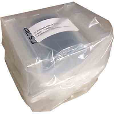
P-Type Silicon Wafers in Wafer Cassettes
UniversityWafer supplies p-type silicon wafers in a wide range of diameters, resistivities, orientations, thicknesses, and surface finishes. Packaging options depend on wafer size, quantity, and cleanliness requirements.
Please let us know the specifications and quantity you need for a quote.
Or Buy Wafers Online .
High-Resistivity P-Type Silicon Wafers for Sensor Fabrication
High-resistivity p-type silicon is commonly used in research involving sensors, detectors, depleted semiconductor structures, MEMS, and other devices that require controlled bulk electrical properties.
One example specification requested for sensor research is:
100 mm P/Boron (100), 3000–4000 Ω·cm, 500 ± 15 µm, SSP, Prime Grade
Specifications can be selected according to the required resistivity, orientation, diameter, thickness, surface finish, and fabrication process.
P-Type Boron-Doped Silicon Wafer Applications
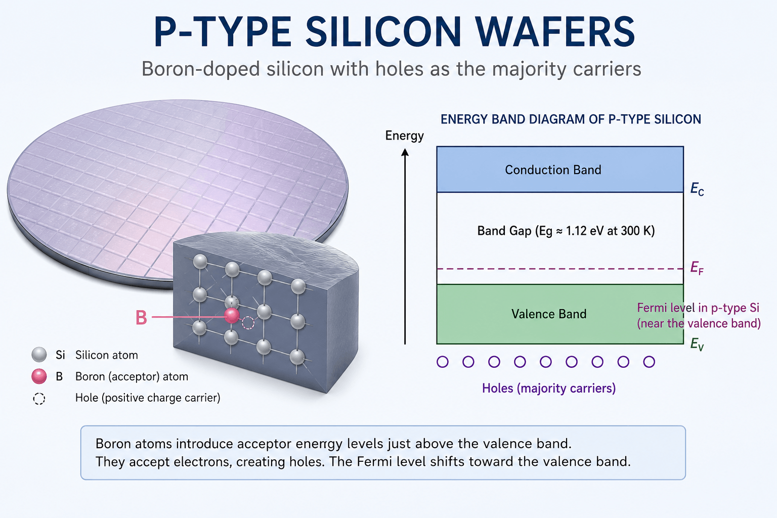
P-type silicon wafers are commonly produced by doping silicon with an acceptor impurity such as boron. Boron has three valence electrons, compared with four for silicon, and introduces acceptor states that increase the hole concentration. Holes therefore become the majority mobile carriers in ordinary p-type silicon.
P-type silicon is available across a broad range of doping concentrations and resistivities. P-type does not automatically mean heavily doped. High-resistivity p-type detector wafers can be lightly doped, while low-resistivity p-type wafers contain much higher acceptor concentrations.
Similarly, crystal orientation and doping are independent specifications. P-type silicon can be supplied in common orientations such as (111) and (100), depending on the application.
Typical uses for p-type silicon include:
- CMOS and semiconductor-device research
- MEMS and microsensor fabrication
- Photolithography and thin-film deposition
- Particle and radiation detectors
- Photodiodes and other junction devices
- Photovoltaic and solar-cell research
- Electrochemical and biosensor experiments
- Epitaxial-device substrates
Epitaxial silicon can also be grown on p-type substrates when a device requires a precisely controlled epitaxial layer thickness, dopant concentration, or resistivity. Whether an epitaxial wafer is appropriate depends on the specific device architecture.
Can P-on-N Silicon Junctions Be Made by Diffusion?
A researcher asked:
I need diffusion-doped p-on-n silicon wafers. Can you provide details on available structures and specifications?
I only require a small quantity, probably around 10 wafers. I would also like to know whether other doping profiles are available for photovoltaic research.
UniversityWafer, Inc. Reply:
Yes. A p-on-n silicon structure can be produced by introducing a p-type dopant, such as boron, into the surface of an n-type silicon substrate. Junction depth and surface dopant concentration depend on the diffusion process, temperature, time, starting substrate, and required device characteristics.
Conversely, diffusing an n-type dopant such as phosphorus into a p-type silicon substrate produces an n-on-p structure. These two configurations should not be treated as interchangeable because they have opposite substrate and emitter conductivity types.
Diffusion profiles can be designed for particular research requirements, but a higher dopant concentration does not automatically mean better device performance. Junction depth, sheet resistance, recombination, contact resistance, carrier lifetime, surface passivation, and the intended device architecture must all be considered.
Example Phosphorus-Diffused P-Type Silicon Wafer
The following is an example of an n-on-p structure because the starting substrate is p-type and the diffused surface layer is n-type phosphorus:
GX82g. 10 — Silicon wafers, SEMI Prime,
4" diameter × 525 ± 25 µm
Substrate: p-type Si:B (100), ρ = 5–10 Ω·cm
TTV < 10 µm, Bow < 40 µm, Warp < 40 µm
One-side polished, backside alkaline etched
Diffused phosphorus n-type surface layer: approximately 500 nm
Nominal dopant/carrier concentration: approximately
5 × 1019 cm−3
Surface-layer resistivity specification: approximately 0.001 Ω·cm
SEMI flats (two)
Packaged in Empak or equivalent cassette
Contact UniversityWafer to confirm current process capability, achievable diffusion profiles, measurement method, quantities, and pricing.
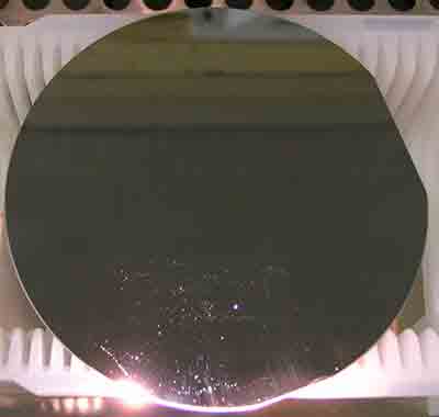
Example image of a silicon wafer surface after a diffusion process:
HF-Etched P-Type Silicon Wafers for Native Oxide Removal
A researcher asked:
Can you provide HF-etched p-type silicon wafers to remove SiO2? Once a silicon wafer is HF etched, how long can it be kept before the surface oxidizes again?
Desired specifications: p-type silicon, (100), approximately 1 Ω·cm, 1-inch diameter, approximately 500 µm thick, quantity 10.
Technical Considerations:
An HF treatment can remove silicon oxide and leave a predominantly hydrogen-terminated silicon surface. However, an oxide-free silicon surface is not indefinitely stable when exposed to water, oxygen, or ordinary ambient conditions. Native oxide formation begins again after the cleaned surface is exposed to an oxidizing environment.
For processes that require a freshly oxide-free silicon surface, an HF-last clean is commonly performed as close as practical to the subsequent processing step. The acceptable delay depends on the process, storage atmosphere, contamination requirements, surface orientation, and required interface quality.
Customers requiring a specific surface condition should specify whether they need native oxide, thermal oxide, an HF-last surface, hydrogen termination, or another cleaning and packaging requirement when requesting a quote.
DOFZ vs. Czochralski Silicon for Detector Applications
Diffusion-Oxygenated Float-Zone (DOFZ) and Czochralski (CZ) silicon differ primarily in their crystal-growth history, impurity concentrations, oxygen content, and achievable electrical properties. These differences can influence their suitability for radiation detectors, sensors, MEMS, and other semiconductor devices.
| Property | DOFZ Silicon | CZ Silicon |
|---|---|---|
| Crystal Growth | Float-Zone material followed by oxygenation | Crystal pulled from molten silicon in a silica crucible |
| Oxygen Content | Oxygen intentionally introduced after FZ growth | Generally higher due to interaction with the silica crucible |
| Purity | Based on high-purity Float-Zone silicon | Typically contains more oxygen and carbon than FZ material |
| High Resistivity | High-resistivity material can be produced | Available over a broad resistivity range |
| Detector Use | Studied extensively for radiation-detector applications | Used in detectors, sensors, power devices, MEMS, and IC fabrication |
Why Oxygen Matters in Detector-Grade Silicon
Oxygen can interact with vacancies and other defects created during irradiation. Because these interactions affect the formation of electrically active defects, oxygen concentration is an important parameter in studies of radiation-damaged silicon.
DOFZ silicon combines the low impurity concentration normally associated with Float-Zone material with intentionally introduced oxygen. CZ silicon naturally contains more oxygen because oxygen enters the silicon melt from the silica crucible during crystal growth.
Radiation tolerance cannot be predicted from oxygen concentration alone. Detector architecture, starting resistivity, thickness, dopant concentration, irradiation particle type, fluence, temperature, and operating voltage must also be considered.
Resistivity and Detector Depletion
High-resistivity silicon is particularly useful for semiconductor detectors because its low net dopant concentration makes it possible to deplete a relatively thick region of the wafer at practical bias voltages.
Detector designers should specify the required conductivity type, resistivity, thickness, crystal orientation, growth method, surface finish, TTV, bow, warp, and oxide condition rather than selecting a wafer based only on whether it is FZ or CZ.
Does P-Type Doping Increase Silicon Conductivity?
Yes. Compared with intrinsic silicon at the same temperature, introducing acceptor dopants can substantially increase electrical conductivity by increasing the concentration of holes.
What Is P-Type Doping?
Pure crystalline silicon has four valence electrons per atom. P-type silicon is produced by introducing an acceptor dopant, most commonly boron.
Boron has three valence electrons. When a boron atom substitutes for a silicon atom in the lattice, it can accept an electron, leaving a mobile hole in the valence band. As a result, holes are the majority carriers in ordinary p-type silicon.
How Doping Affects Conductivity
Semiconductor conductivity depends on both carrier concentration and carrier mobility. Increasing acceptor concentration generally increases the hole concentration and decreases resistivity. At high doping concentrations, however, carrier mobility and other material properties also change, so the relationship is not perfectly linear.
| Property | Intrinsic Silicon | P-Type Silicon |
|---|---|---|
| Majority Carrier | Neither | Holes |
| Electron / Hole Concentration | Approximately equal | Hole concentration exceeds electron concentration |
| Common Dopant | None intentionally added | Boron |
| Fermi Level | Near the intrinsic level | Moves toward the valence band as acceptor concentration increases |
P-Type Silicon Wafers Available Online
UniversityWafer supplies boron-doped p-type silicon in multiple diameters, resistivities, orientations, thicknesses, and surface finishes.
Current inventory changes frequently. Use the links below to check available specifications and pricing:
- 2-Inch (50.8 mm) Silicon Wafers
- 3-Inch (76.2 mm) Silicon Wafers
- 100 mm (4-Inch) Silicon Wafers
- 150 mm (6-Inch) Silicon Wafers
- 200 mm (8-Inch) Silicon Wafers
Thin P-Type Silicon Wafers
Thin silicon substrates are used in MEMS, sensors, flexible-device research, semiconductor packaging, detector development, and other applications where reduced substrate thickness is required.
View Thin Silicon Wafers Available Online
Custom thinning, polishing, dicing, and other wafer-processing services may also be available for research quantities. Contact UniversityWafer with your required starting wafer and final thickness specifications.
P-Type Silicon Wafer Resistivity
P-type silicon is available across a very broad resistivity range. Resistivity should not be confused with the simple classification of a wafer as p-type. A wafer can be either lightly or heavily p-doped.
In general, increasing the electrically active acceptor concentration decreases resistivity. Very low-resistivity material is useful when high electrical conductivity is required, while high-resistivity p-type silicon is commonly requested for detectors and other devices requiring a low bulk dopant concentration.
Float-Zone silicon is particularly useful when high purity and high resistivity are required. Czochralski silicon is also available over a broad range of resistivities and is widely used throughout semiconductor manufacturing.
How Is P-Type Silicon Identified?
A silicon wafer cannot reliably be identified as p-type or n-type simply by looking at its surface. Conductivity type is an electrical property determined by the dominant electrically active dopants and resulting majority carriers.
Common methods used to characterize semiconductor conductivity type and electrical properties include Hall-effect measurements, hot-probe measurements, spreading-resistance measurements, and four-point-probe resistivity measurements, depending on the information required.
Historically, wafer flats were also used to encode certain orientation and conductivity information according to particular wafer standards. However, flat geometry should not be treated as a universal method for identifying every modern silicon wafer.
P-Type vs. N-Type Silicon
The fundamental difference between p-type and n-type silicon is the type of majority mobile charge carrier.
| Property | P-Type Silicon | N-Type Silicon |
|---|---|---|
| Majority Carrier | Holes | Electrons |
| Typical Silicon Dopant | Boron | Phosphorus |
| Dopant Function | Acceptor | Donor |
| Fermi-Level Shift | Toward the valence band | Toward the conduction band |
Does P-Type Doping Change the Silicon Band Gap?
Ordinary p-type doping does not turn silicon into a fundamentally narrow-band-gap semiconductor.
At room temperature, crystalline silicon has a band gap of approximately 1.12 eV. Introducing boron creates acceptor states near the valence-band edge and changes carrier concentration and the position of the Fermi level.
At very high dopant concentrations, effects such as band-gap narrowing can occur. This is different from saying that all p-type silicon has a smaller fundamental band gap than n-type silicon.
Where Is the Fermi Level in P-Type Silicon?
The Fermi level is the electron chemical potential and determines the statistical probability that available electronic states are occupied.
In intrinsic silicon, the Fermi level lies close to the middle of the band gap. Adding acceptor dopants increases the hole concentration and shifts the Fermi level toward the valence-band edge.
In n-type silicon, donor doping shifts the Fermi level toward the conduction-band edge.
The exact Fermi-level position depends on temperature, dopant concentration, dopant ionization, and whether the semiconductor is in the nondegenerate or degenerate doping regime.
What Is a P-N Junction?
A p-n junction forms when p-type and n-type semiconductor regions meet. Electrons diffuse from the n-type region toward the p-type region while holes diffuse in the opposite direction.
This carrier diffusion creates a depletion region containing ionized donors and acceptors and establishes a built-in electric field. The resulting junction behavior is fundamental to semiconductor devices such as diodes, photodiodes, solar cells, transistors, radiation detectors, LEDs, and integrated circuits.
What Is Avalanche Breakdown?
Avalanche breakdown can occur in a sufficiently reverse-biased semiconductor junction when the electric field becomes strong enough for charge carriers to gain substantial kinetic energy.
These energetic carriers can create additional electron-hole pairs through impact ionization. The newly generated carriers are accelerated by the electric field and can create additional carriers, producing avalanche multiplication.
Avalanche breakdown does not occur at one universal voltage such as 5 V. Breakdown voltage depends on junction geometry, dopant concentrations, electric-field distribution, semiconductor material, and device design.
Silicon Wafer FAQs
What Is Silicon Wafer TTV?
Total Thickness Variation (TTV) is the difference between the maximum and minimum wafer thickness measured across the wafer. Low TTV can be important for lithography, bonding, MEMS fabrication, polishing, and other precision processes.
What Is Silicon Wafer Surface Roughness?
Surface roughness describes microscopic variations in wafer surface height. Values may be reported as Ra or Rq/RMS, depending on the measurement method. Because these metrics are not identical, the measurement parameter and instrument should be specified when requesting a particular surface finish.
Can You Buy a Single Silicon Wafer?
Yes. UniversityWafer specializes in supplying researchers, universities, laboratories, startups, and engineers with small quantities of silicon wafers, including individual wafers when available.
What Is Silicon Wafer Reclaim?
Silicon wafer reclaim is the process of removing previously deposited films, coatings, residues, or surface damage so that suitable wafers can be cleaned, polished, and reused.
Reclaimed wafers are commonly used for equipment qualification, process development, monitoring, testing, and other applications that do not require new prime-grade material.
Can Silicon Wafers Be Custom Processed?
Silicon wafers can be processed using services such as thinning, polishing, dicing, oxidation, nitride deposition, metal deposition, and other microfabrication-related processes depending on the requested specifications.