I need 1" Si wafers to be masked and used as witness plates in a metal deposition system. Wafers will then be used or profilometer measurements. What is most cost effective solution for this need?
1 Inch Silicon Wafers Used For Profilometer Measurements
A Wafer Fab Process Group Team Leader requested a quote for the following.
Reference #111172 for specs and pricing.
Get Your Quote FAST! Or, Buy Online and Start Researching Today!
Thin Silicon Wafers Checked RMS Checked With Profilometer
A corporate scientist requested a quote for the following.
We need the following thin silicon wafers.
1. Item: Silicon wafers
2. Thickness: 100 um
3. Roughness (rms): <10A {vendor
should mention the technique used
for determining the roughness}
4. Dia: 3 inch
5. Single side polished
6. P-type or n-type
7. Orientation: <100> = 0.5
8. Resistivity: 50-100 ohm cm
9. TTV: <3 um
10. Bow warp: < 30 um
The wafers should be in good condition (broken pieces will not be accepted). The rms roughness will be checked using stylus
profilometer/atomic force microscopy and it should be less than or equal to the specified value. The orientation will be
checked using XRD technique.
Reference # for specs and pricing.
What is Profilometer?
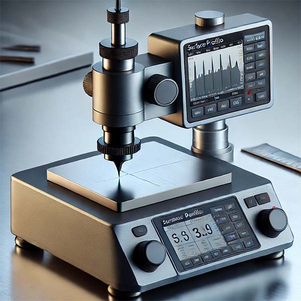
A profilometer is a precise measuring instrument used to assess the surface profile and topography of a material. It measures surface roughness, texture, and features like step heights or thin film thickness. Profilometers are often used in industries like semiconductor manufacturing, materials science, and engineering to evaluate the smoothness or irregularity of surfaces.
There are two main types of profilometers:
Contact Profilometers: These use a stylus that physically moves across the surface of the material to trace its contour. The vertical displacement of the stylus is measured to calculate the surface profile. These are very precise and can measure tiny surface variations but may cause wear on soft surfaces.
Non-Contact Profilometers: These use optical methods, such as white light interferometry or laser scanning, to measure the surface without touching it. Non-contact profilometers are faster and avoid damaging delicate surfaces.
In your context, profilometers could be useful for measuring the thickness and uniformity of coatings, such as the thin films you are working on.

What Is A Stylus Profilometer?
A stylus profilometer is a type of contact profilometer that uses a physical probe, or stylus, to measure the surface topography of a material. The stylus, typically made from a hard material like diamond, is drawn across the surface to trace its contour. As the stylus moves over surface features like ridges or valleys, it vertically deflects in response to changes in height, and these deflections are recorded to create a profile of the surface.
Key Features of a Stylus Profilometer:
-
Contact-Based Measurement: The stylus directly touches the surface, making it ideal for precise measurements of step heights, roughness, or thin film thickness.
-
High Precision: Stylus profilometers can detect very fine surface features, with vertical resolution as small as a few nanometers.
-
Surface Profile: The vertical movement of the stylus is translated into electrical signals, which are processed to produce a graph or 3D image of the surface profile.
-
Applications: These are commonly used in semiconductor fabrication, MEMS, coatings, and material science to evaluate surface roughness, film thickness, and pattern quality.
-
Limitations: Since it requires physical contact with the surface, the stylus profilometer may not be suitable for soft or delicate materials that can be scratched or deformed. It also tends to be slower than non-contact methods.
For your work with coatings, especially if they are thin or delicate, a stylus profilometer might provide excellent precision for measuring thickness and surface roughness, but you would need to ensure the material isn't too sensitive to physical contact.
How Do You Test Substrates Thin-Film Sress Using A Profilometer?
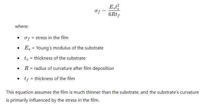
To test thin-film stress on substrates using a profilometer, you typically measure the curvature of the substrate before and after film deposition. By analyzing the change in curvature, you can calculate the stress in the thin film. This process is based on the Stoney equation, which relates the film stress to the curvature of the substrate.
Steps for Measuring Thin-Film Stress with a Profilometer:
-
Initial Curvature Measurement (Before Deposition):
- Measure the curvature of the bare substrate using the profilometer.
- The substrate is usually flat, but if there is any initial curvature due to pre-existing stress or bowing, this must be captured.
- The profilometer scans the surface of the substrate, and the data provides a baseline for comparison after the film is deposited.
-
Film Deposition:
- Deposit the thin film (e.g., metal, oxide, etc.) onto the substrate. This deposition can induce stress due to differences in thermal expansion coefficients, lattice mismatch, or deposition conditions.
-
Second Curvature Measurement (After Deposition):
- After the thin film is deposited, use the profilometer again to measure the curvature of the substrate.
- The film deposition may cause the substrate to bend (either concave or convex), depending on whether the stress is tensile or compressive.
-
Calculate the Curvature Change:
- Calculate the difference between the initial curvature (before deposition) and the final curvature (after deposition).
- This change in curvature is crucial for determining the thin-film stress.
-
Use the Stoney Equation:
- Apply the Stoney equation to calculate the film stress based on the measured curvature change:

- Apply the Stoney equation to calculate the film stress based on the measured curvature change:
- This equation assumes the film is much thinner than the substrate, and the substrate's curvature is primarily influenced by the stress in the film.
Important Considerations:
- Film and Substrate Properties: You need to know the material properties of the substrate (e.g., Young's modulus and Poisson's ratio) to use the Stoney equation effectively.
- Profilometer Resolution: The profilometer must be sensitive enough to detect the small curvature changes caused by the thin film, which can be in the micrometer to nanometer range.
- Film Thickness: Profilometers can also measure the thickness of the thin film, which is required for the stress calculation.
This method is widely used in semiconductor fabrication, MEMS, and materials science to evaluate how stress in thin films could affect the performance or reliability of devices.
