Silicon Solar Cell Breakthrough in Performance
Silicon Solar Resistively Bounded Subcells
A breakthrough for enhancing the performance of silicon solar. We are excited to introduce a breakthrough in the science of silicon photovoltaics, called Resistively Bounded Subcells (RBS). This new approach to photovoltaics requires no additional factory equipment or materials and it has sweeping applications across the solar industry.
Get Your Quote FAST! Or, Buy Online and Start Researching Today!
First Commercially Available Product the Configurable Current Cell (C3)
he first commercially available product based on the RBS innovation is the Configurable Current Cell (C3). C3 reduces silver costs by 3% on the sunny side of a PV cell and up to 5% on the rear side of a PV cell, increases overall module power by 2-3 watts, and delivers higher lifetime energy in the field. In late 2019, the US Department of Energy recognized the promise of C3 by awarding Solar Inventions nearly $1 million as the first-ever recipient of the American Made Solar Prize.
For a 300-MW PERC cell and module manufacturer, C3 creates nearly US$1 million in value through this 3% reduction in silver and additional 2-3 watts per 60-cell panel. Because C3 strengthens the electrical divide for current inside a cell, heat-related issues are lowered, which reduces warranty claims and fire risks.
For cell manufacturers, C3 requires only small changes in metalization print patterns and selective doping. Manufacturers can implement C3 by working with Solar Inventions to modify their print screens and make a small set of additional easy and risk-free changes to their production lines. For modules, C3 configures the subcells in parallel to a cell’s traditional busbars and therefore requires no changes to the tabbing and stringing of panels, making it quick and easy to introduce into an existing module manufacturer.
C3 mimics some of the benefits of split-cells and half-cells without the costs associated with physically cleaving the cells. C3 will power even more exciting applications as the industry continues increasing the size of cells. By subdividing the current in larger cells, C3 can reduce the resistive losses that increase as cell sizes grow past six inches.
Product roadmap — the Configurable Voltage Cell (CVC)
Enhanced Silicon Solar Cell Performance
UniversityWafer, Inc. and it's partner introduce resistively bounded subcells:
The lowest-cost method of increasing
PV efficiency while improving safety
and energy production
Breakthrough new electrical cell architecture enables PV manufacturers to gain immediate benefits with existing production equipment and processes, with no risk.
- Mainstream panels and cells — more power, increased safety, reduced materials, and more lifetime energy production.
- Solar shingles for residential rooftops — tremendously simplified wiring and design, along with higher reliability
- Lanterns and solar home systems for low-income countries — higher voltage solar cells reduce electronics and complex module assembly
- Space applications — more flexibility in designing modules and more redundancy with fewer power electronics required
- Large format wafers — cells greater than 6 inches will benefit from reduced current loss due to electrical heat dissipation for elevated current flow
- Cell directly powers electronics without lossy voltage conversion (like cell phones or chargers)
Invented by Solar Invention’s Chief Scientist, Dr. Benjamin Damiani, RBS creates multiple electrically isolated subcells on a single silicon wafer, using equipment and processes that already exist in most of the world’s solar manufacturers. RBS works with 95% of all silicon cell architectures including monocrystalline, polycrystalline, PERC, HJT, and bi-facial. While scientists have long understood the idea of subcells (also called
“monolithic cells”), creating them required specialized processing and was prohibitively limited in efficiency. Now, any manufacturer can immediately improve their profits, fabrication losses, and warranty returns — all without risk to throughput or quality.
How Does it Work?
By connecting subcells in series within a single cell, the cell’s voltage is increased proportionately. For example, a traditional cell might produce 0.65 volts at 9 amps, whereas a CVC cell with two subcells will produce 1.3 volts at 4.5 amps. This can be readily scaled up to any number of subcells — CVC has been successfully fabricated and tested with up to 12 subcells at UNC Charlotte and the Georgia Institute of Technology, generating more than 5 volts from a single, unbroken cell.
The applications of CVC are exciting and broad:
- Solar shingles with greatly simplified wiring requirements, greatly reducing the cost of residential solar
- Higher-voltage panels that can be wired in parallel, which simplifies inverter designs and reduces external power electronics
- Lower-cost single cells that directly power electronics, like phone chargers and solar lanterns for low-income countries.
CVC is still in laboratory development. Commercial pilots are anticipated for late 2020 or early 2021. C3 and CVC are complementary and can be used together, laying the foundation for rapidly commercializing a range of brand-new functionality and price-points in the solar marketplace.
The Science Behind Resistively Bounded Subcells
The patent-pending breakthrough behind C3 creates isolated changes in cell resistance. This is done through a combination of metalization laydown changes and, in some cases, a post-metalization lasering step. Dr. Damiani’s research has uncovered specific metalization patterns, both on the top and bottom of cells, that together create precise areas of higher cell resistance, which in turn are used as electrical boundaries around the hybrid subcells. These subcells exhibit characteristics that have previously only been possible with exotic wafer processing techniques or physical cleaving such as half-cells.
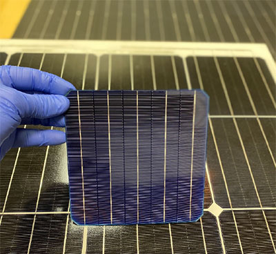
C3 creates value across six areas:
1. Reduced metal consumption: 3%-5% reduction in silver
One of the most expensive components of fabricating a solar cell is the use of silver as electrical contacts on the front and/or rear side of a solar cell. The pattern used by C3 to create subcells results in a net silver savings proportional to the number of busbars on the cell. A three-busbar “H” pattern reduces silver consumption and and a six-busbar pattern reduces it further. See Figure 2 for a control chart of silver deposition during a sample pilot production of a five-busbar cell design. In certain cell architectures, the reduction in silver materials is matched by reduction in aluminum.
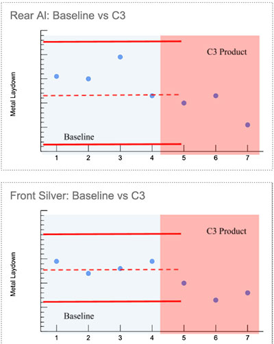
Figure 2. Process control chart measured during a 12-hour
shift in a >500 MW solar cell fabrication plant, where the only change to production was a shift to C3 silver metalization on the front and rear side of the wafer. Both the front and rear side metalization were reduced by ~3% for a five-busbar “H” pattern.
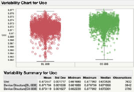
2. Improved cell efficiency: 0.1%-0.2% absolute efficiency boost The reduction in silver contact area acts to reduce the recombination velocity for metal on the silicon surface, resulting in a 1 mV-5 mV boost in open circuit voltage at the cell level. Figure 3 shows a data snapshot for C3 performance compared to the baseline group during the same production run for the silver savings shown in Figure 2.
The reduction in silver consumption also directly translates into less front metal shadowing, allowing more optical transmission into the bulk silicon for absorption and electrical current creation. Figure 4 shows the corresponding boost in short circuit current due to ~3% less front metal shadowing.
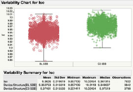
mono PERC cells fabricated during the production run described in Figure 1.
3. Improved Cell-to-Module Ratio (CTM) The improved open-circuit voltage and higher short-circuit current results in higher module-level power because the module fill factor (FF) is unchanged compared with a standard PV cell, which in turn reduces CTM losses due to the higher open-circuit voltage (VOC) for the C3 enhanced modules. The CTM benefits require no changes to the existing stringing and encapsulation equipment. Figures 5 and 6 show module level data for the same production run referenced in this white paper. Taken together, the higher VOC in C3 modules combined with an unchanged FF raises the overall CTM and power output of a module. Similar results have been obtained from multiple mid- to large-scale module manufacturers.
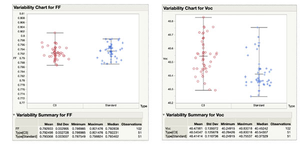
Figure 6. Increased open circuit voltage (~2mV per cell) for C3 enhanced mono PERC cells fabricated during the production run described in Figure 1
4. Improved safety
The C3 electrical boundaries between each subcell slightly isolate the flow of current across the wafer, reducing current concentration around defects or small optical obstructions. The initial product release for C3 offers a mild improvement over baseline solar cells. Our next generation incorporates technology that substantially improves panel safety while decreasing power dissipation during a shading event.
5. Improved energy production compared to half-cells
The creation of subcells on a single silicon wafer without physically cleaving the solar cell maintains a smaller wafer perimeter compared to the wafer area of the individual solar cells. Each time a solar cell is cut in half, the ratio of the perimeter to the surface increases. This results in non-ideal diode effects and higher edge recombination velocity for individual “Half Cells.” The C3 technology does not utilize a physical cleave and avoids the increased perimeter issue. Note that while C3 offers benefits over half-cells, it is entirely compatible with half-cells, offering improved power and safety benefits.
6. Reduced losses in large wafer sizes
The International Technology Roadmap for Photovoltaics (ITRPV) shows a trend toward larger wafer sizes. They are increasing past the standard 156mm, with factories starting to use wafers up to 210mm per square side. This increased size raises the cells overall short circuit current, but simultaneously increases the electrical heat loss (I^2R), reducing power. The most popular remedy is to cleave the cell into two or more physical pieces. This requires expensive equipment upgrades,increased material losses, and reduced
cell efficiency to contribute to module power. Subcells and the C3 technology allow an additional layer of flexibility that permits these increasingly larger formats to reduce their virtual size without the need for cleaving.
