Substrates and Services Provided by UniversityWafer, Inc.
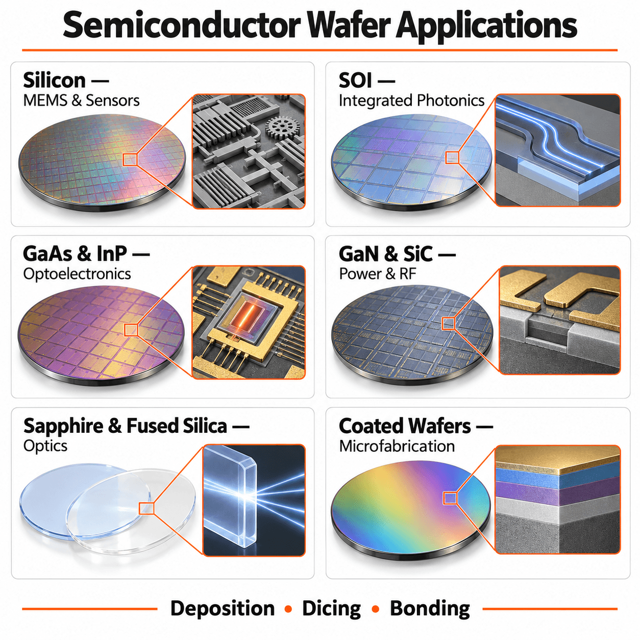
UniversityWafer supplies semiconductor wafers, optical substrates, and custom wafer processing for research and fabrication. Explore silicon wafers, SOI wafers, III-V substrates, and silicon carbide, or review our wafer processing services.
Request a quote with your desired material, diameter, orientation, thickness, dopant, resistivity, coating, finish, quantity, and any processing requirements. We can help identify suitable stock or custom substrate options.
Get Your Quote FAST! Or, Buy Online and Start Your Research Today!
Aluminum
Glass Substrates
Quartz and Transparent Substrates
III-V Substrates
Semiconductor Wafers and Research Substrates
Choose a wafer by its electrical, optical, thermal, and process requirements. We supply these material families for research and prototype fabrication:
- Silicon wafers: P-type, N-type, undoped, float zone, and epitaxial silicon options, depending on the required diameter and specification.
- III-V compound semiconductors: gallium arsenide (GaAs), indium phosphide (InP), and gallium nitride (GaN) for electronic and optoelectronic research.
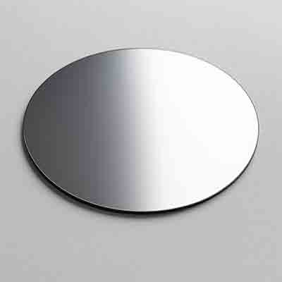 Silicon carbide (SiC) is a separate wide-bandgap compound semiconductor.
 - Silicon-on-insulator (SOI) wafers: An engineered silicon device layer above a buried oxide layer for microelectronics, MEMS, and photonics.
- Graphene and 2D materials: Research materials for sensors, electronics, and nanostructure development.
- Glass, quartz, and specialty substrates: Borofloat 33, BK7, fused silica, sapphire, germanium, and ITO-coated substrates for optical and device research.
Specifications such as wafer diameter, orientation, resistivity, layer thickness, and polish should match the intended fabrication process. Availability and lead time vary by material and configuration.
Wafer Processing Services
Our wafer processing services support custom research and prototype projects:
- Thermal oxide and silicon nitride: Dielectric films for insulation, masking, and passivation.
- Metal deposition: Films such as aluminum, gold, and titanium for contacts, electrodes, and coatings.
- Wafer dicing: Cutting wafers into specified sample or die sizes, subject to material and thickness.
- Wafer bonding: Combining compatible wafer surfaces for device structures and research assemblies.
- Wafer reclaim: Cleaning, stripping, and refinishing suitable used silicon wafers for reuse.
- Custom wafer specifications: Select diameter, orientation, dopant, resistivity, thickness, surface finish, or coating for your project.
For a processing quote, include the starting substrate, target film or final dimensions, tolerances, quantity, and any testing requirements. Contact us to discuss options and timing.