
Silicon Wafer Bonding Services
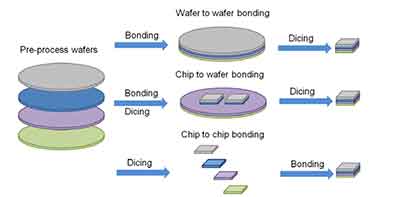
Wafer bonding is a process used to attach one wafer to another. The two wafers need to be placed in a horizontal position and the topography of the two wafers might differ dramatically. Therefore, the package assembly process needs to take these variations into account. However, there are several ways to accomplish this. Here are the most common methods.
UniversityWafer, Inc. can help you with all your bonding needs.
Get Your Quote FAST! Or, Buy Online and Start Researching Today!
What Is Wafer To Wafer Bonding?
What is wafer to wafer bonding? This is a process used to attach a wafer to another. The wafers need to be placed in a horizontal position. In addition, the topography of the two wafers might differ dramatically. Therefore, the package assembly process needs to take these variations into account. However, there are several ways to accomplish this. Here are the most common methods.
Wafer to wafer bonding is a packaging technology that ensures hermetically sealed encapsulation. Its  diameters range from 100 mm to 200 mm, or about four to eight inches. In the early days of the microelectronics industry, wafers were smaller, about one inch in diameter. The bonding technology used must match the substrate and gaseous atmosphere.
If the wafers are not identical, they are bonded by either dipping in buffered HF or cleaving with a diamond scribe. A wafer pair that is not bonded will have voids and is unable to function properly. The other way to test a bond is to use a razor edge inserted into the space between the two. A dicing saw will then be used to cut the pair apart.
The different types of bonding are based on the materials being used. In some cases, the wafers are bonded to temporary carrier substrates, but this process is usually done after they have been debonded from them. While this method is more commonly used in semiconductor applications, it is also preferred in some manufacturing processes. It offers higher throughput, as well as a simpler way to align the different layers of the semiconductor.
When a wafer is bonded to a temporary carrier substrate, it must be debonded and then bonded again. In some cases, the process is front-attached, which allows for frontside processing. In other cases, the carrier is back-attached, which allows for backside processing to be performed. In other cases, the carrier is attached to a permanent carrier and is separated afterwards.
Before the bonding process, the wafers must be properly prepared. This is the only way to achieve the best results. This process is often used for high-tech devices, but it is important to note that the process sequence is different for different types of semiconductor wafers. It is important to make sure the substrate is suitable for the processing method you are using. It is also important to consider the type of carrier you are using. If you're using front-attached carriers, you can process the backside while the carrier is attached to the backside.
The process itself depends on the type of wafers. If you're using temporary carriers, you can attach the wafers to the carriers using a glue or another material. You can then separate the wafers once you have bonded them. Once you've bonded the two pieces of the stack, the process can begin. In some cases, it's necessary to process both sides of the stack.
Wafer to wafer bonding is done by ensuring that the two layers of the semiconductor are properly aligned. This is necessary for the process to be successful, otherwise, the components will slide off. The process is also critical for the quality of the final product. If the two layers don't align correctly, you won't be able to get the desired results. But it does require precision and high-quality products.
When using the eutectic state, the metals that are bonded are in liquid phase, resulting in a planarized surface. The liquid state of the interface provides good tolerance for particle size and topography. The materials are permanently connected. The process is a crucial step in semiconductor manufacturing. The process can be costly and may result in errors. By choosing the right material and the right adhesives, you can create a high-quality product.
This process requires two wafers to be bonded together. It has many benefits, including high flexibility. It also allows for high-bandwidth memory. Unlike the previous method, the eutectic method is low-temperature. And it can be used to make a semiconductor product, which has a high-performance price. It's a great way to reduce costs in manufacturing and improves manufacturing.
How Do I Bond to Borofloat Glass Wafers?
onding wafers are commonly used in the electronics industry for the purpose of bonding conductive or non-conductive polymers or metal oxides into a substrate. These wafers are also known as fiber-optic wafers. They are designed to be vacuum dried while still being capable of conducting electricity. This bonding process produces devices that are highly conductive of both electricity and light. To make the bonding process to work, there are three kinds of wafers: Boron, silicon and borofloat glass.

Bending glass is accomplished with the aid of the present invention. In the present invention, the wafers have a flat top surface and are aligned along the two lateral sides of the flat top surface, thus forming a strong but flexible wafer layer. The wafers are made from a solid, yet thermoplastic, material which permits a large area of contact between the bottom surface and the substrate. The method of bonding includes dipping the wafer into a source of a polymer solution, which allows the solution to adhere to the surface of the wafer while bonding it with the help of a dipole moment between the two solutions.
The semiconductor diodes that are used for the purpose of completing the present invention comprise the major part of the bonding wafers. Silicon is commonly used as a semiconductor because of its ability to maintain electronic charge. The silicon is also responsible for aiding the electronic transition and therefore forms an essential part of the semiconductor materials used for the purpose of completing the present invention. Silicon is used as a semiconductor in the form of silicon dioxide or silica, which is often formed as a result of the formation of mountains after a long period of pressure buildup. Silicone has high electrical and mechanical properties that make it highly suitable for use as a semiconductor by bonding the wafers with silicon oxide.
Various types of metal films surfaces are also used for bonding. A metal-coated bond is often considered as a superior bonding method. A substrate having metal coating is soaked in a chemical bath, which is then sprayed with a bonding agent such as polymer. The metal films surfaces are bonded to one another using a nitrile sponging pad. This bonding process is called nitride adhesives.
Another method that can be used for bonding is to use a rotary bonder. This machine consists of a rotating screw that applies continuous rotating torque to a bone. It applies such a force that the wafers are forced to align themselves in a straight line. The principal reason for selecting this method is that it gives a uniform, clean and very strong bond. The most common of rotary bonders available today is the rotary clicker. A rotary clicker has a small round ring at its center; it has two flat contact pads which, when clicked, pull the two wafers into alignment.
Another method for creating a permanent wafer bonding is through the use of an inertial sensor. An inertial sensor is used because the strength of bonding between two semi-conductor materials depends on their relative positions. When two semi conductors are placed next to each other, their relative positions cause them to emit electromagnetic waves that are detected by the sensor. When the sensor senses these waves, the relative positions change and the required strength of bonding between the two semi conductors are automatically increased.
Bending, compressing, rolling and sliding are some other methods of bonding. These methods are used in industries such as aerospace, automotive, electronics, power generation, communications, medical devices, military applications etc. Some of the devices manufactured using these processes are computers, cameras, TV sets, radio transmitters and receivers, watches, hand tools, industrial machines and other items. There are certain types of wafers that are used for bonding, and the method of bonding depends on the type of wafer and the required alignment. The most common types of wafers that are used for bonding are:
A wafer control unit 40 is a device used in bonding the wafers and one or more substrates to the substrate. The wafer control unit 40 is designed to allow the user to adjust the properties of the bonding. One can use the various methods of bonding to create a variety of functional devices. This article is meant to provide an overview of the various processes of bonding and also to describe some of the different types of wafers.
Silicon Wafer Bonding
Semiconductor wafer bonding has been a topic for many years and in recent decades we have seen numerous innovations in wafers and bonding techniques. Wafer-to-waverage has become a semiconductor technology that enables high-performance semiconductors and low-power semiconductor devices. [Sources: 10, 11]
Another advantage of this invention is the ability to use existing silicon wafer manufacturing facilities and still achieve the great performance that is possible on silicon wafers. Without the use of silicon wafer bonding technology, such market success for MEMS products would be unlikely. [Sources: 1, 9]
The market for semiconductor wafer bonding systems is directly dependent on the growth of the electronics market, as most of the silicon wafers that are passed through bonding are installed in the form of solar cells, solar cells and other electronic devices. Due to pressure from the solar cell industry, low ASP's on silicon wafers have not met the demand for high-performance and cost-effective PV cell products. [Sources: 7, 10]
In recent years, as bond-based applications have moved into mass production, wafer bonding has proven to be a valuable MEMS manufacturing technology. With the introduction of wafers that can connect and create 3D architectures, and applications that use wavelength integration, it has become very attractive. However, new challenges have been raised in the watherbonding process, as the bonding functionality of wafer electronics has shifted from predominantly unprocessed surfaces to mechanically processed wafers. [Sources: 0]
Unfortunately, one of the limitations of using SiC is that the wafer size is much smaller than with conventional silicon wafers. The width and length of silicon carbide wafers is smaller in diameter than silicon carbide, but the width of silicon carbides increases with the size of their surface. [Sources: 9]
Rieutord et al. assume that the gravitational force between the two silicon wafers in hydrophobic bonds can be limited to van der Waal's forces in a first approach. This adhesive force allows the polishing of the silicon carbide wafer due to the presence of a small amount of water on the surface and the formation of an adhesive bond. [Sources: 2]
After reaching the eutectic temperature, the solder liquefies on the surface of the wafer, where it comes into contact with silicon carbide. [Sources: 11]
This technique limits the amount of crystal defects introduced into the silicon wafer during the bonding process, as essentially no mechanical force is required to initiate the bonded effect of the wafers. However, after the wafer compounds, an additional, single-stage cleaning step - wafer cleaning - is often used to remove any particles trapped on the surface after cleaning the wet bench or wafer bonding system. This includes processing the surface in such a way that the edges are not well bonded, and connecting them to the contact surface. If you feel confident enough to manipulate this step and see that the binding works better, you can expect your wafers to connect during this process. [Sources: 0, 5, 8, 13]
The anodic bond is also used to join two silicon wafers with a thin, sputter- backed glass layer. This high-temperature step is performed at a higher temperature than the omitted step, so that the bonds become stronger. Bonding silicone wafers to glass using removable UV adhesives helps to strengthen the wafer and protect it from damage. During the bonding process, pressure builds up in the heat-treated wafer configuration, which forms hydrogen gas bubbles in the dispenser substrate and separates them. [Sources: 1, 3, 8, 12]
The silicon-bound surface is highly ammonophobic during plasma processing, and the wetting angle of ammonia drops on the silicon is lowered at 120 adeg. The surface area of gallium nitride is about 30 degrees, which indicates the degree of motility achieved. In contrast, the surface bonds of silicon-bound surfaces are around -30ADg, suggesting that they are not at the same temperature as the wafer. [Sources: 5]
Most silicon features are formed first, and the final carrier wafer consists of a layer of handle wafers that are bonded before and after. The layer on the handle of each wafer is glued to the layer above it, which is then glued back to the tip by gluing the wearer on the top of the wafer. [Sources: 4, 6]
The surface of the treated wafer is then contacted with a fully bonded silicon-nitride interface to form a bonded hybrid semiconductor structure with a surface area of about 1.5 micrometers or about one tenth of a millimeter. The intermediate bond structure is annealed and forms a layer of intermediate structures consisting of a silicon oxide layer and a nitric oxide surface, which is driven by heating the intermediate structure during the annealing process. Then the interbound structures are cancelled again, this time with the final carrier wafers, until the silicon and nitrite interfaces are fully bound. [Sources: 5]
Direct bonding is also called silicon fusion bonding, which uses silicon-to-silicon fusion compounds. It is mainly used to manufacture high-performance silicon wafers such as semiconductors, photovoltaics and solar cells. This usually requires the use of a silicon oxide layer and a nitrogen oxide surface and a high degree of lead edge binding between the silicon and nitrite interfaces. [Sources: 1, 3, 10]
Sources:
[0]: https://www.prosysmeg.com/Papers/Aligned-Fusion-Wafer-Bonding.html
[2]: https://iopscience.iop.org/article/10.1088/2043-6262/1/4/043004
[3]: https://www.ques10.com/p/26877/write-short-note-on-wafer-bonding-1/
[4]: https://www.eejournal.com/article/20170228-backside-photonics/
[5]: https://patents.google.com/patent/US8796054
[6]: http://www.semiconductor-today.com/news_items/2016/jul/smart_260716.shtml
[7]: https://www.prnewswire.com/news-releases/global-semiconductor-silicon-wafer-markets-2018-2023-overview-of-direct-bonding-surface-activated-bonding-plasma-activated-bonding-and-anodic-bonding-300953012.html
[8]: http://www.freepatentsonline.com/6159824.html
[9]: https://www.google.com/patents/US5349207
[10]: https://www.esticastresearch.com/media-release/wafer-bonding-system-market/
[11]: https://www.sensorprod.com/news/articles/2010-03_wdpi/index.php
[12]: https://www.syagrussystems.com/3m-wafer-support-system
[13]: https://cleanroom.byu.edu/waferbonding
What is Anodic Wafer Bonding?
Anodic bonding is a semiconductor manufacturing process that requires atomic contact between two substrates. In this process, anodic bonds are made by placing the wafers in a chuck and applying an electric potential of several hundred volts. The result of the process is an oxygen-rich layer on the interface of the wafers and silicon dioxide. Anodic bonding is a very effective process for semiconductor manufacturing and can be used for a variety of applications.
The process begins with atomic contact and spreads to the edges of the two wafers. In anodic bonding, glass and silicon are placed above one another. In order to create an anode, an electrode is used. This can be a needle, a full-area cathode electrode, or a chuck. During the process, the glass acts as the anode while the chuck is the cathode.
To perform anodic bonding, two clean substrates are placed in a bond chamber. One is glass, and the other is a material that forms an oxide. Both surfaces are contacted with a high-voltage anode and an electrostatic field. The voltage induces mobile sodium ions to migrate toward the glass' negative contact. The oxygen atoms then bond with the silicon surface. Anodic bonding is irreversible. The glass substrate must be free of contamination and have a good electrical contact.
What is Direct Wafer Bonding?
One of the common techniques in the manufacturing of electronic components is direct wafer bonding. In this process, chemical bonds are formed between molecules of a substrate. The adhesion strength of direct wafer bonding is typically low at room temperature. The maximum strength of the bonds is achieved by thermal annealing at a high temperature. In order to get the maximum bond strength, the surface needs to be highly pristine.
The technology uses a wide range of polymers and adhesives for bonding. It is commonly used in microelectronics. It is also relatively low-cost and simple. In addition, the resulting wafer-bonds have a low melting temperature. This makes them compatible with standard integrated circuit materials. This method is a good choice for large-scale production of electronic components. In addition, it can be used to manufacture photonic devices.
The process uses a liquid-phase eutectic alloy for the bonding layer. This process is more durable than direct wafer bonding because it is less sensitive to scratches or other surface irregularities. The polymer adhesive bears the force necessary to hold the two substrates together, and ensures even temperature distribution across the bonded stack. As a result, eutectic bonding can also reduce residual stresses associated with thermal cycling.
What is Adhesive Wafer Bonding?
What is Adhesive Wafer Bonding? This process involves bonding two semiconductor wafers together. The adhesive is usually spin-coated and cured to adhere them together. The adhesive may be thick on the front side of the wafer to protect circuit components from damage, or thin on the back side to prevent bowing. It is an ideal process for flexible electronics and is also a viable alternative to tape mounting.
There are two methods for adhesion. Thermal debonding uses a single-layer adhesive that is applied at room  temperature. A plasma pretreatment removes organic contamination from the wafer surface. Another method is hydrophilic bonding, which uses a thin layer of water on a glass carrier. This method is effective because it is low-temperature and can be done without high-temperature equipment.
Chemical debonding dissolves the adhesive, but is slow for large wafers, because it only reaches the edges of the wafer. Chuan-An Cheng, an engineering student from Taiwan's National Chiao Tung University, discovered a process called "debonding" that uses ultra-thin intermediate layers. This technique allows for 99% bonding yield and 4.8 MPa of bonding strength.
This process is most commonly used in the semiconductor industry and is the preferred method of bonding wafers with chips. It also reduces the chances of cracking and warping by eliminating the need for expensive tools. In addition, this process is more reliable, with higher throughput and reduced waste. So, if you're in the industry for making semiconductors, adhesive wafer bonding could be the right solution for your manufacturing needs.
What is Silicon Fusion Bonding?
The Use of Silicon Fusion Bonding in MEMS Devices
A silicon based MEMS device can benefit from the application of silicon fusion bonding. The process can be performed with the use of a pressure-assisted fusion bonding process. The silicon substrates can be flat and relatively clean. However, a few parameters need to be controlled, such as Ra, which is required for a successful synthesis. The wafers must also be in intimate contact with each other for the process to be effective.
A Suitable Process For Crack-Free Wafer Boding With Silicon
A crack-free wafer can have multiple layers of defects and require a particular type of process. In this article, we discuss crack-free wafer boding processes for silicon and gallium nitride. You will also learn about other materials such as sapphire and al2o3.

HDP-SiO2, Thermal Oxide, PE-Si2N4, Graphene, Silicon
Gallium Nitride
This insulator demonstrates unique optical and electrical properties, including an excellent aqueous stability. Its aqueous stability and biocompatibility make it a strong candidate for a variety of chemical and biological applications. Additionally, gallium nitride is highly amenable to molecular modification. For example, the surface of gallium nitride was functionalized using a peptide that promotes PC12 cell adhesion. The peptide was attached to the surface by covalent methods and by olefin metathesis.
This process was initially developed to fabricate crack-free n-type semiconductors, which have low-dimensional resistance and large free carrier concentrations. Using silicon as the base substrate, gallium nitride can be used for crack-free wafer boding with silicon. The n-electrodes are metallic-filled through-holes. The n-electrodes are placed on a temporary substrate, which allowed for thinning of the silicon substrate. The n-electrodes were removed by a wet chemical etch that utilized hydrofluoric-nitric-acetic acid.
GaN is an ideal candidate for crack-free wafer boding. The material is a great choice for high-performance devices. This process is also inexpensive and suited for low-temperature manufacturing in a Si wafer fab. Its low substrate cost and large diameter make it ideal for a number of applications. Further, the GaN/Diamond composite has the potential to replace silicon in extreme environments.
Sapphire (Al2O3)
A key benefit of this process is the ability to create crack-free wafers. This is achieved by using sapphire as a substrate and a silicon mask. During this process, the silicon wafer is cleaned by deionized water before being bonded to the sapphire. The resulting hBN layer can be as thin as the silicon native oxide, or as thick as the sapphire native oxide.
To prepare the samples for direct bonding with silicon, two sapphire pieces were cut along their cross sections. A piece was etched to a depth of 4 mm, with the other piece etched with a shallow cylindrical cavity. The minimum pressure load for direct bonding was set to 14.6 MPa using a custom furnace with a high initial pressure. The cross-section was coated with a thin gold film to image the etched pieces. The resulting images were analyzed using a scanning electron microscope and are shown in Figure 8a.
The sapphire sensing cavity is 5 mm in diameter and 4.8 um deep. In the optical interference between the two sapphire wafers, multiple colored Newton rings appear. These interference rings indicate a tight bonding between the two sapphire wafers. The sensor structure also lacks interference rings outside of the central cylindrical cavity. Sapphire is a suitable process for crack-free wafer boding with silicon.
This study demonstrated that ALD-deposited amorphous Al2O3 films can be fabricated at 200degC, and characterization by XRD and EDS showed a stable O/Al ratio. Surface morphologies and roughness values were similar. SE analysis indicated that the film thickness increased with ALD cycles at a rate of 0.1 nm/cycle. In addition, a UV-VIS transmittance spectrum revealed a uniform band gap, and no significant fluctuation was observed.
Another technique that is capable of producing crack-free silicon wafers is anodic bonding. This technique involves placing the silicon and glass wafers above one another and applying an electrode. This electrode may be a needle, full-area cathode electrode, or a chuck. The glass acts as the anode, and the silicon acts as the cathode.
Another method of crack-free silicon wafer boding involves the use of abrasive particles. Al2o3 particles can be adsorbate on abrasive particles and can form network structures under high shear rates. The strong hydrogen bonding of silica particles triggers a shear-thickening effect. Increasing temperature also affects the slurry's viscosity, and this is reflected in a Stribeck curve.
Silicon Wafer
Direct wafer bonding is a common manufacturing method, wherein the bonded surfaces are controlled by surface preparation and wafer flatness. Crack propagation is modeled using a spectral scheme, and the effect of surface roughness was studied by varying fracture-toughness on the bond interface. The energetics of crack propagation depend on the local variation in surface properties. Compared with unpatterned silicon wafers, patterned silicon is tougher than unpatterned ones.
In order to achieve a crack-free silicon wafer, the first step of silicon wafer bonding is to bond the surface of the wafer with a substrate. The process produces cavities in the wafer, which are crucial to subsequent high-temperature bonding. In particular, the presence of oxygen inside the cavity can be detrimental to subsequent bonding because it reacts with the silicon surface and creates a partial vacuum. In other words, the pressure in the cavity equals that of 20% air.
A suitable process for crack-free silicon waper boding involves three steps: the hydrating step, the liquid-phase eutectic alloy bonding layer, and the high-temperature anneal. The anneal temperature is the final step of the bonding process. The higher the temperature, the higher the bond strength. The process also involves a final step called a high-temperature annealing, which is performed between 800 and 1200C.
Wafer Bonding
Developing a crack-free wafer bonding process involves a number of factors. The following is a detailed description of the process. These factors are important to the development of high-quality, crack-free wafers. These processes are applicable to a wide range of devices, including micromechanics. They are a powerful process that can be used to bond silicon wafers together.
The semiconductor industry has developed several bonding processes for integrating different materials. It has become a critical tool in manufacturing advanced devices. This technique has several unique properties. The adhesive strength, power dissipation, and crosstalk must be minimal for accurate device structures. Other requirements include achieving good junctions. Silicon fusion bonding is one of these methods. Silicon-nitride-based bonding is another method.
Regardless of the method used, crack-free wafer bonding requires a pristine environment. The surfaces of the wafers are cleaned and hydrated. The process then contacts the wafers with one point. Surface attraction acts between the two wafers, causing them to adhere together as a wave. However, multiple points of contact may trap air pockets between them. Depending on the type of bond, multiple points of contact can also cause problems.
Light Emiting Diode (LED)
The advantages of led bodied silicon wafers over other boding processes include crack-free fabrication and higher quality. This technique allows for new design freedom, such as stacking different materials. It also enables fabrication of material combinations that are impossible to realize through conventional epitaxial growth. Led boding can be used for both conventional and advanced silicon wafer boding processes.
This process can produce crack-free silicon wafers because of the low-melting-point of the adhesive used in the process. It is also compatible with standard integrated circuit materials. This makes it a good choice for high-volume production of electronic components, including high-performance photonic devices. Further, the process does not restrict downstream processing. Further processing steps can be carried out at higher temperatures and under high vacuum, without any problem.
Direct silicon wafer bonding is a promising process for manufacturing of three-dimensional microelectronic devices. However, the process does have its limitations, and crack-free silicon wafers are not yet commercially available. It is possible to achieve crack-free silicon wafers through a crack-free boding process, although the bond quality decreases with increasing surface roughness.
The light-emitting diode process combines the copper substrate with an AlN-based metal reflector. It is the only process to eliminate the absorptive silicon substrate and introduce a single layer of gold metal between the electrodes. The resultant copper sub-mount has an improved p/n and n-bonding surface. It also eliminates the electro-shading losses.
The light-emitting diode device is comprised of two main layers: the exposed metal layer and the metal substrate. The metal layer is composed of at least one metal, such as Pt, Rh, Ru, or Au. Then, the metal layer is covered by a conductive sub-mount substrate. The sub-mount substrate is connected directly to the p-ohmic contact electrode and the metal pad that is used as the heat sink area.
The nitride semiconductor layer has a strong polarization field, resulting from strain in lattice-mismatched structures. This strain can cause emissions to shift in a red/long wavelength direction. A lower strain causes less QCSE and higher internal quantum efficiency. It may also lead to shifts in peak emission wavelength. In the copper-based LED, there was no wavelength shift.
Bonding Substrates
Suitable processes for crack-free wafer boding are important for semiconductor fabrication. These processes make use of silicon dioxide, which aids the transition of an electrical current from one state to another. Several processes can bond different types of semiconductor wafers, but all have the same basic steps. A suitable process for crack-free wafer boding with silicon can be found for a variety of high-tech devices.
IR imaging methods are widely used for characterization of wafers. They measure the crack length and determine the bond toughness of the material. The bond strength depends on the crack length, and uncertainties in this parameter can be large. In order to minimize crack length uncertainties, a suitable process for crack-free wafer boding with silicon should include controlled HF and temperature. Here are a few methods for crack-free wafer boding with silicon:
Direct silicon bonding is the preferred method for SOI-wafers and for SOI-with-cavities. Direct silicon bonding requires higher surface smoothness than anodic bonding. Moreover, the process requires high-temperature treatment and extreme surface quality with minimal chemical contamination. Hence, a suitable process for crack-free wafer boding with silicon should meet the requirements of the semiconductor industry.
Silicon-to-Silicon Wafer Bonding
A scientist requested a quote for the following:
"I would like to have a quote for a bonded silicon wafer where I can have chromium-gold-chromium films between two silicon wafers. Layers would be as follow: (Silicon wafer{500 um}-chromium{20-30 nm}-gold {30-40 nm}-chromium{100 nm}-silicon wafer {100-150 um}). the thiner wafer need to be double-side polished."
Diameter: 4 inch
Type: N-Type
Dopant: (not important)
Orientation: <100>
Resistivity(Ohm-Cm): lower better
Thickness (um): already mentioned
Polish: DSP
Grade: Test or Prime
Quantity: 5 (although it depends on the price, if it was expensive, I might go for lower like 3)
If this type of wafer worked for me and was ok, I would like to bond another thin wafer to the other side of the 500 um wafer, where at the end of the day I will have three wafers, 100 um thin-500 um thick-100 um thin. Films between them would be the same as what I explained (shown below). Even if by eliminating the thinner chromium layer the whole thing gets easier, I'm ok with that (number 2 in the picture below).
If you could make the number 1 or 2 in the picture below and it worked for me, I would like to have the same configuration for double-sided bonded wafer later (number 3).

UniversityWafer Quoted the following. Please reference RFQ#251159 for pricing
bonded silicon wafer
Layers would be as follow:
(Silicon wafer{500 um}-chromium{20-30 nm}-gold{30-40 nm}-chromium{100 nm}-silicon wafer{100-150 um}). the thiner wafer need to be double-side polished.
Diameter: 4 inch
Type: N
Dopant: (not important)
Orientation: <100>
Resistivity(Ohm-Cm): lower better
Thickness (um): already mentioned
Polish: DSP
Grade: Prime
Bonding Wafers for Low Noise Detectors
A scientist requested the following quote:
"150 mm diameter, undoped (or very weakly doped P-type), 100, as high resistance as possible. Need 10-25 wafers depending on pricing (please provide pricing o different quantities). We need to be able to use a Germanium (Ge) wafers with our ASML stepper, so a standard notch on the wafer indicating the wafer orientation would be necessary.
We will use the wafer for making low noise detectors, so low background doping is preferred, and the wafer will be used for wafer bonding, so we need a good flatness and smooth surface ( a_rms < 1 nm desired)."
UniversityWafer, Inc. Quoted GeOSi wafers. Reference #257125 for pricing.
- Germanium wafers 6 inch , low doping (resistivity > 10 ohm-cm).Single side polishing,thickness ~675um. Qty. 25pcs
- Germanium wafers 4 inch , N-type low n-type Sb doping (resistivity n/s).Single side polishing.,thickness ~525um.Qty. 25pcs
Our Application is for Photonics After Wafer Bonding Process
A scientist from a large university requested a quote for the following:
"We are looking for silicon carbide wafer for project application. I would like to get 4inch or 6inch 4H-HPSI SiC wafer quotation. Double side polished for SiC wafer. Any thickness is okay for us. What we care about is roughness and warpage. It is better roughness less than 1nm, warpage less than 15um. If not, please recommend the best one. Also, we would like the HPSI one instead of doping one. HPSI, roughness and warpage can meet our requirement, right? It is so good. Our application is for photonics after wafer bonding process.
UniversityWafer, Inc. Quoted:
Silicon carbide wafer for project application. 4inch 4H-HPSI SiC wafer,Quantity is 2 pieces. (6 inch also available.)
Double side polished SiC wafer.
Thickness 500+/-25um
Surface roughness: Si-face roughness <0.5nm
C-face roughness <1.0nm
Wafer warpage: <15um
HPSI SiC Wafer, Undoped SiC
Reference #262560 for pricing.