Requested specifications:
- Material: Single-crystal GaP
- Orientation: (110)
- Dimensions: 5 × 5 mm or 10 × 10 mm
- Thickness: Approximately 800 µm–1 mm
- Excitation wavelength: 1030 nm
- Quantity: 2 pieces
Reference #269809

Gallium phosphide (GaP) is a III-V compound semiconductor used in photonics, optoelectronics, nonlinear optics, terahertz (THz) experiments, photoelectrochemistry, nanotechnology, and semiconductor materials research.
Single-crystal GaP substrates are available with selected crystal orientations, thicknesses, electrical properties, dopants, and surface finishes. Researchers may require nominally undoped, high-resistivity, n-type, or p-type material depending on the optical or electronic requirements of the experiment.
A device researcher requested small (110)-oriented GaP substrates for an optical experiment using a 1030 nm excitation source.
Requested specifications:
Reference #269809
A university researcher requested a thin, nominally undoped GaP crystal for experimental research.
When an exact specification is unavailable, researchers can also request the closest available thickness, wafer diameter, or diced piece size.
Reference #268345
Get Your Gallium Phosphide Wafer Quote FAST! Or, Buy Wafers Online and Start Researching Today!
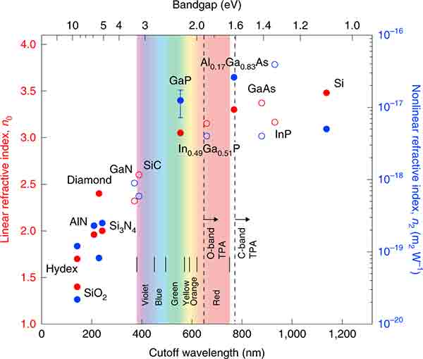
GaP combines semiconductor behavior with useful optical properties. At room temperature, gallium phosphide has an indirect fundamental band gap of approximately 2.26 eV. Because photon energies below the absorption edge are not sufficient to produce fundamental interband absorption, GaP can transmit light over useful wavelength ranges when absorption from defects, impurities, free carriers, and surface effects is sufficiently low.
GaP also has a relatively high refractive index and useful nonlinear optical properties. Together, these characteristics make high-quality GaP crystals interesting for nonlinear optics, integrated photonics, electro-optic measurements, frequency conversion, and terahertz research.
Gallium phosphide is used in terahertz (THz) research because of its nonlinear optical and electro-optic properties. Depending on the experimental configuration, GaP crystals can be used for THz generation or electro-optic detection of ultrafast THz fields.
(110)-oriented GaP is commonly requested for these experiments. Crystal thickness can influence phase matching, bandwidth, absorption, and interaction length, so researchers often specify the thickness according to the laser wavelength and desired THz response.
A university researcher requested a GaP sample for THz generation using a 1030 nm optical source.
One suitable research configuration consisted of a 25 × 25 mm nominally undoped (110) GaP substrate, approximately 1 mm thick, with both surfaces polished.
Double-side-polished surfaces are particularly useful when an optical beam must enter and exit the substrate through polished faces.
Single-crystal GaP substrates are also used for research involving nanostructured surfaces, semiconductor interfaces, photonic structures, catalysts, and light-driven chemical reactions. Crystal orientation, doping, surface preparation, and defect density can influence both fabrication and experimental behavior.
For example, researchers have used Zn-doped p-type (100) GaP with polished, epi-ready surfaces for studies involving patterned semiconductor interfaces and light-driven chemistry.
Surface preparation is particularly important for nanoscale research because roughness, contamination, native surface chemistry, and crystal defects can influence subsequent processing and interface properties.
Gallium phosphide offers a useful combination of electronic, optical, electro-optic, and nonlinear optical properties. Its suitability depends on the specific device or experiment, but important characteristics include:
Gallium phosphide is a binary III-V compound semiconductor composed of gallium and phosphorus. Bulk single-crystal GaP has the zinc-blende crystal structure and a lattice constant of approximately 5.45 Å at room temperature.
Unlike direct-band-gap semiconductors such as GaAs, bulk GaP has an indirect fundamental band gap. This reduces the probability of direct radiative electron-hole recombination and affects how GaP is used in light-emitting devices.
GaP can be prepared with different electrical characteristics through controlled doping and crystal growth. Depending on the required application, researchers may select:
Electrical specifications such as resistivity, carrier concentration, mobility, and dopant species should be considered when selecting material for a specific experiment.
GaP has an established history in visible light-emitting diodes. Although its indirect band gap makes light emission less efficient than in many direct-band-gap III-V semiconductors, suitable dopants and device structures can introduce efficient radiative recombination pathways for selected visible wavelengths.
Historically, GaP has been particularly important for green, yellow-green, and red light-emitting devices, depending on doping and device design.
Modern GaP research extends beyond conventional LEDs into nanophotonics, nonlinear optics, integrated photonics, semiconductor interfaces, and nanoscale optical structures.
GaP wafers and crystals are used across a range of research applications, including:
Providing complete specifications helps identify the most appropriate gallium phosphide wafer or crystal for your research.
Gallium phosphide (GaP) is a III-V compound semiconductor used in optoelectronics, nonlinear optics, terahertz (THz) research, photonics, light-emitting devices, and semiconductor materials research. GaP has an indirect fundamental band gap of approximately 2.26 eV at room temperature, with higher-energy direct optical transitions that are important to its optical behavior.
UniversityWafer supplies gallium phosphide wafers in undoped, n-type, p-type, and high-resistivity configurations with selected crystal orientations, thicknesses, surface finishes, and electrical specifications for research and device development.
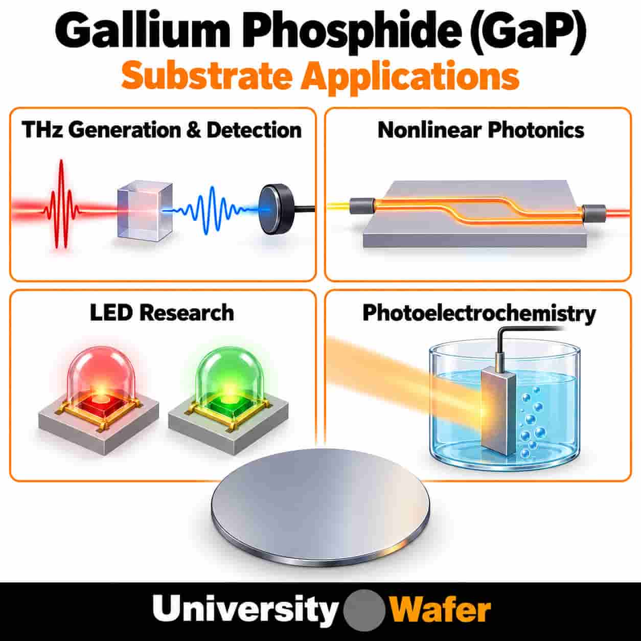
Gallium phosphide is used in electro-optic sampling, terahertz generation and detection, and nonlinear optical experiments. Its nonlinear optical response and useful transparency over portions of the visible and infrared spectrum make appropriately prepared GaP crystals useful for ultrafast optical and THz research.
For these applications, researchers may require high-resistivity or nominally undoped material, specific crystallographic orientations, controlled thickness, and double-side-polished surfaces. The optimum specification depends on the wavelength, optical geometry, propagation direction, and experimental configuration.
A postdoctoral researcher requested thin, high-resistivity GaP material for electro-optic research.
Reference #226295
Another researcher requested GaP wafers for THz field generation and detection.
One evaluated specification included 2-inch, (110)-oriented, high-resistivity GaP with both surfaces polished.
Reference #271387
The appropriate electrical properties of a GaP substrate depend on the experiment or device. Researchers should select material according to parameters such as resistivity, carrier concentration, dopant, mobility, optical absorption, orientation, and surface finish rather than relying only on labels such as "undoped" or "semi-insulating."
Nominally undoped GaP should not automatically be assumed to be electrically intrinsic. Residual impurities and native defects can influence carrier concentration and conductivity, so researchers should specify the required electrical properties directly whenever possible.
GaP substrates may be selected according to crystal orientation, conductivity, dopant, resistivity, carrier concentration, mobility, etch pit density, thickness, and surface finish. Available inventory varies, so researchers should confirm the specifications required for their experiment.
Common specification options may include:
Because GaP has a room-temperature fundamental band gap of approximately 2.26 eV, it can absorb photons with energies above its band-gap threshold, including a portion of the visible spectrum. This has led to research involving photoelectrochemistry, photocatalysis, solar-energy conversion, semiconductor-liquid interfaces, and light-driven chemical reactions.
The efficiency of these systems is not determined by band gap alone. Surface chemistry, doping, carrier lifetime, recombination, interface energetics, crystal quality, and catalytic layers can all strongly affect photoelectrochemical performance.
Researchers have used single-crystal p-type GaP substrates to study semiconductor interfaces for visible-light-driven chemical reactions. One research configuration used Zn-doped (100) GaP with measured electrical and crystal-quality specifications.
Reference #225200
GaP has a long history in visible light-emitting devices. Because its fundamental band gap is indirect, radiative recombination is less efficient than in direct-band-gap III-V semiconductors such as GaAs or GaN. Nevertheless, appropriate doping and device structures have enabled GaP-based LEDs, particularly in portions of the visible spectrum.
GaP is also used as a substrate and semiconductor material for research involving optical emitters, detectors, nonlinear optics, and integrated photonic structures.
Gallium phosphide is attractive for nonlinear photonics because it combines a relatively high refractive index with useful nonlinear optical properties and transparency across relevant wavelength ranges. These characteristics have motivated research into GaP waveguides, resonators, photonic crystals, frequency-conversion structures, and nanoscale optical devices.
High-quality crystalline material, smooth surfaces, carefully fabricated interfaces, and low optical loss are important when GaP is used in photonic structures.
GaP is also investigated in nanoscale forms including nanowires, nanophotonic structures, membranes, and photonic-crystal devices. At these dimensions, geometry and surface properties can strongly influence optical, electronic, and biological interactions.
Characterization methods used for GaP nanostructures and wafers can include Raman spectroscopy, photoluminescence, electron microscopy, atomic force microscopy, electrical measurements, and optical spectroscopy.
The combination of semiconductor, optical, electro-optic, and nonlinear properties makes GaP substrates useful across several research areas.
To request a GaP wafer or substrate, provide as many of the following specifications as possible: