N-Type FD Silicon-on-Insulator
A PhD candidate requested a qutoe for the following:
Do you have any n-type Fully Depleted SOI wafers with a device layer thickness less than 300nm?
I'm interested in buying some FD SOI wafers or pieces.
The device thickness should be less than 300nm, and the doping is n-type with a resistivity of between 0.1 and 10 ohm.cm.
I can buy one or two wafers (100mm) or any size pieces.
Please let me know if you have any stocks available.
Reference #159180 for specs and pricing.
Get Your Quote FAST! Or, Buy Online and Start Researching Today!
Fully Depleted SOI Wafers for RF Applications
A wireless communications researcher requested the following:
Have you the possibility to provide FD SOI with top Si < 100 nm (intrinsic & heavily p doped)for our Radio Frequency research?
With thick BOX of > 2 um.
If yes, could I have a quote for a few Wafers ?
(200 mm in diameter?)
Reference #230910 for specs and pricing.
Fully Depleted Silicon-on-Insulator's Promising Performance
FD-SOI technology is a promising technology for low-voltage VLSI circuits. It is a great alternative to traditional bulk devices and offers a number of advantages. The unique characteristics of FD-SOI transistors make them suitable for the production of small-scale electronic components. With this, the market is poised for rapid growth. If you are in the market for high-performance semiconductors, this report is essential.
268498
SIMOX Silicon-on-Insulator Wafers in Stock
SOI Item #G4P-017-01 - 100mm P/B (100) 500um14-22 ohm-cm Device 340nm, Oxide 1000nm UNIBOND Prime Grade
(50 wafers left)
(75 wafers left)
SOI Item #G4M-005-01- 100mm P/ B(100) 500um 14-22 ohm-cm Device 340nm, Oxide 400nm UNIBOND Monitor Grade
SOI Wafer Special
SOI - Can't buy many wafers? We can quote you just one wafer.
For example
150mm SOI P/B (100) 625um 1,000 ohm-cm
Device 200nm
Oxide 1,000nm
Don't buy ten if you don't have to!
November Special
- 8" SOI with device layer 50nm thick
-Top Si: p-type/<100>/8.5-11.5 ohm.cm
-Box:0.2um thick
-Handle Si wafer:p-type/<100>/725um thick/15 ohm.cm
The price is
-$590.00/ea for 5 wafers.
-$690.00 each for one
While the supply lasts!
Below are just some Soitec Silicon-on-Insulator Wafers that we have in stock
| Item |
Dia |
Typ/Dop |
Ori |
Res ohm-cm |
Handle |
Device nm |
Oxide μm (or nm) |
| 2327 |
25mm sq |
P/B |
(100) |
14-22 |
625 |
500 |
3 |
| 2377 |
150mm |
P/B |
(100) |
14-22 |
675 |
100 |
200nm |
| 2415 |
150mm |
P/B |
(100) |
13.5-22.5 |
625 |
500 |
3 |
| 2265 |
200mm |
P/B |
(100) |
9-16 |
725 |
145 |
135 |
| 2266 |
200mm |
P/B |
(100) |
9-16 |
725 |
190 |
150 |
| 2551 |
200mm |
P/B |
(100) |
1-20 |
725 |
70 |
2,000nm |
| 2268 |
300mm |
P/B |
(100) |
9-16 |
775 |
50 |
145 |
What is Fully Depleted Silicon-on-Insulator (FDSOI) Wafer?
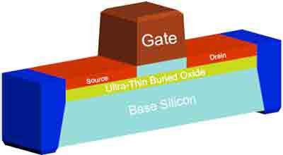
FDSOI is a semiconductor process based on the planar process. It uses a thin layer of SiON/TiN to produce a semiconductor device. The gate stack is made of two layers of 2.5-nm thick SiON/TiN. The device is also characterized by its length from source to drain. The FDSOI device is a highly efficient and cost-effective semiconductor.
The FD-SOI transistor is shown in Figure 2. The transistor is fabricated on a 28nm FDSOI wafer, demonstrating its structure. According to the research report, the FD-SOI technology demonstrates several important advantages for advanced nodes. Among them is superior electrostatic control of the gate, an efficient body biasing, and a good balance between power consumption and performance.
A fully depleted SOI device is a hybrid device that combines a semiconductor substrate (p-doped silicon) with a buried oxide layer ("BOX"). This FD-SOI device consists of a base-layer FET and a thin layer of silicon. The underlying structure of the FD-SOI wafer is a multi-layered structure made of a thin, highly conductive layer of silicon.
The Fully Depleted Silicon-on-insulator technology is a planar process technology. This technology can help in creating chips with low power and better performance. The FD-SOI technology is also a good fit for a number of applications. It is a good choice for a variety of industries. With its many advantages, it can help in the manufacturing of semiconductors. The FD-SOI technology is a great alternative for those in the semiconductor industry.
How is FD-SOI Different than Bulk CMOS Silicon?
FD-SOI is a semiconductor technology that is different from a bulk CMOS silicon. The difference between FD-SOI and bulk CMOS is the extra layer of oxide. The extra oxide layer facilitates the manufacturing process. The extra layer of silicon also enhances the effective electron mobility of the transistor. Besides, it provides an excellent platform for multi-Vt integration. This research addresses various FD-SOI technologies, including the thin BOX and planar FD-SOI.
Fully-depleted silicon-on-insulator transistors are coated with a layer of gadolinium oxide, a practical converter material. The company claims that its new transistor technology is able to detect the smallest amounts of neutrons. Although these devices are expensive, they can provide good sensitivity. In addition to the sensitivity, the Fully Depleted Silicon-on-Insulator technology is a viable option for many electronic applications.
FD-SOI, also known as ultra-thin silicon-on-insulator, is an alternative to bulk-silicon used in CMOS devices. FD-SOI transistors have shallow channels and an optimized channel structure to increase the ability of the gate to remove carriers when it switches off. This reduces the off-leakage current, which is problematic as chip designs become increasingly dense and smaller.
Is FDSOI Cost Effective?
FDSOI is a new technology that can significantly decrease the cost of semiconductor manufacturing and bring down the threshold of Moore's law. FDSOI uses a thin silicon layer between five and 20 nanometers (nm) in order to create transistors with a smaller width. In addition to this, the thickness of the SOI layer is not larger than the depletion width of the device.
What Research Uses Fully Depleted Silicon-on-Insulator (SOI) Substrates
Fully Depleted Silicon-on-Insulator (FD-SOI) substrates are used in various research and practical applications, primarily in the field of semiconductor technology. Here are some of the key areas where FD-SOI is utilized
- Low-Power Electronics: FD-SOI is highly valued in the design and manufacture of low-power electronic
 devices. Its properties enable the creation of transistors that operate efficiently at low voltages, which is crucial for battery-powered devices like smartphones and tablets.
- High-Performance Computing: Due to its excellent electrical properties, FD-SOI is used in high-
 performance computing applications. It helps in creating processors that can handle intensive tasks while maintaining energy efficiency.
- Radio Frequency (RF) Applications: FD-SOI substrates are ideal for RF circuit applications, such as
 those found in wireless communication devices. They offer better signal integrity and lower power consumption compared to traditional bulk silicon substrates.
- Automotive Electronics: The automotive industry benefits from FD-SOI technology, especially in the
 development of smart sensors and control units that require low power consumption and high reliability under varying temperature conditions.
- IoT Devices: The Internet of Things (IoT) devices, which often operate on low power and require long
 battery life, can greatly benefit from FD-SOI technology. This includes sensors, smart home devices, and wearable technology.
 Research in Semiconductor Physics: FD-SOI substrates are also used in academic and industrial research to study advanced semiconductor physics and develop new electronic components.
- Space Applications: Due to their enhanced tolerance to radiation compared to bulk silicon, FD-SOI
 devices are finding applications in space electronics, where reliability and resistance to harsh environmental conditions are crucial.
- Neuromorphic Computing: FD-SOI is being explored in the field of neuromorphic computing, which
 aims to mimic the neural structure of the human brain in hardware, for its potential to create energy-efficient and high-speed computing systems.
- Flexible Electronics: The thin layer structure of FD-SOI makes it suitable for use in flexible electronic
 applications, where it can be used to create bendable and foldable electronic devices.
In summary, FD-SOI technology is pivotal in advancing various high-tech fields, particularly where energy efficiency, performance, and miniaturization are critical factors.