
Polycrystalline Silicon Wafers
We have a large selection of Polycrystalline Si wafers. Please let us know what specs and quantity you would like us to quote?
A researcher requested a quote for the following:
"I am looking of Polysilicon/SiO2/Si wafer with polysilicon thickness of ~50nm."
UniversityWafer Replied:
Polysilicon layer is Undoped Polycrystalline Silicon deposited by sputtering on the SiO2 layer over the polished side. The Polysilicon is undoped and likely to measure as n-type, but user can dope it by any one of standard doping techniques. Polysilicon layer is offered 100nm thick, because thinner layers are likely to exhibit lack of uniformity. Unpolished wafer back-side will be covered by Thermal Oxide and possibly some polysilicon deposited on the back-side unintentionally.
Reference #252333 for specs/pricing.
Send us your specs and start your research today!
Below is just one recent order!
Si Wafer
Polycrystalline
3", 350um, DSP
Quantity: 25 wafers
Get Your Quote FAST! Buy Online and Start Your Research Today!
What is Defect Segmentation
Polycrystalline silicon wafers inhomogeneous background makes it difficult for researchers to automatically segment defects.
A computer can't know what a defect on a silicon wafer looks like. So it needs to be told what a defect looks like. The computer has to be taught. It has to be shown lots of examples of what a defect looks like, and it has to be shown lots of examples of what the silicon wafer background looks like. And then, after the computer has been taught what a defect looks like, and what the silicon wafer background looks like, the computer can look at a new image and tell whether it contains defects or not.
Calculating Surface Roughness of Polycrystalline Silicon Wafers
The mathematical model used to calculate surface roughness is as follows:
1. The cutting depth of abrasives is discretized as the cutting groove and wire profile during the sawing process.
2. Material removal mode of abrasives is judged by cutting depth.
3. According to the calculation nodes closest to the sawn surface, the wafer surface profile and roughness along the feed speed direction are calculated. 4. The results showed that the relationships between surface roughness and feed speed Vf, wire speed Vs and their ratio Vf /Vs satisfied power functions. 5.
Finally, the calculation result of surface roughness was used to generate a 3D surface morphology of wafer.
Slicing Photovoltaic Polycrystalline Silicon with Diamond
Polycrystalline silicon is the most commonly used material for silicon solar cells. The slicing process is the first mechanical processing step of battery cells, the quality of sawn surface affects the cost of subsequent processes such as texture making, also affects the breaking strength of battery cells and the photoelectric conversion efficiency and other performances. In this paper, polycrystalline silicon sawing experiments are carried out, and the effects of main process parameters, such as the workpiece feed speed, the wire moving speed, the ratio of the workpiece feed speed to the wire moving speed, and the sawn workpiece size, on the surface morphology and roughness Ra of the photovoltaic polycrystalline silicon slice are analyzed. Orthogonal experimental method was used to analyze the primary and secondary order and positive and negative effects of various factors on surface morphology and surface roughness, the optimum process parameters were obtained, and the wear morphology and mechanism of wire were analyzed. The research results show that: within the range of process parameters studied in this paper, the surface morphology of polycrystalline silicon slices shows a comprehensive effect of material ductility and brittleness removal.
Learn Solar Energy | Fabricating Crystalline Silicon
What is Polysilicon?
What is polysilicon? This chemical is used in the semiconductor industry at both the component and microscale levels. It is manufactured using different methods, including ion implantation, zone melting, and Bridgman techniques. The following is a description of some of the most common types of polysilicon, their uses, and the processes required to produce them. The report provides a comprehensive overview of the market for this material.
Polysilicon is the primary component of solar cells. It is a natural material, with high crystalline structure. It is extracted from quartzite, a medium-grained rock with an approximate 90-99% purity. This mineral is used in the production of electronic devices, as well as in the manufacture of electronics. It is the most abundant mineral in the world, and is also used in semiconductor manufacturing. It is a highly versatile material that is highly resistant to radiation, making it useful in many applications.
In 2015, China dominated the global polysilicon market, with a 27% share. Europe and the USA followed, with Korea taking up the remaining 7%. The two largest polysilicon suppliers in the world are GCL Group, Hemlock Semiconductor, and OCI. Other leading suppliers in the industry include Sichuan Yongxiang, TBEA, and REC Silicon. However, the demand for polysilicon in the semiconductor industry has remained relatively high despite the pricey nature of these materials.
Polysilicon is a common material used for solar cells. Its use has increased dramatically in the last decade. In the last twenty years, the global market for polysilicon has grown from 13,600 MT to 28,000 MT. Its demand has increased by 167 times since 2005, and the solar PV industry is growing fast. By 2010, the imbalance between supply and demand had been corrected, and polysilicon prices dropped to a level comparable to that of the industrialized world. In 2014, the global demand for the material reached 420,000 MT, which is the lowest for polysilicon.
As the solar PV industry continues to grow, the demand for polysilicon is growing rapidly. The global market for polysilicon is expected to reach USD 19400 million in 2027, a 10.8% CAGR. The global market for polysilicon is projected to grow by 2020. In addition to cell phones, it is also used in the production of solar panels and in energy storage. It is also used in semiconductors and in solar panels.
The process for producing polysilicon involves a chemical reaction that releases hydrogen and phosphine gas. This process deposits the polysilicon in a layer on a semiconductor wafer. When the chemical reaction is completed, it creates a thin film of polysilicon and a polycrystalline film on the semiconductor wafer. The silicon is then cast into the solar cell. The final result is a multicrystalline silicon film.
One of the prime reasons for the growth of the Polysilicon Market is the growing demand for semiconductor chips. The manufacturing of semiconductors is the most crucial process for the production of solar panels. By 2020, companies can create up to 30,000 to 35,000 tons of polysilicon. This is a huge amount of polysilicon. It is produced by a process called exfoliation. The method is a very efficient one.
China dominates the global market for polysilicon. The US and Europe account for the other 18% of the market. The UK and Japan are the two other major markets for this material. The global market for polysilicon is estimated at $10 billion. In terms of volume, China produces about five tons of the material per year. In the United States, it is worth a few billion dollars. The global industry is driven by several factors.
The largest polysilicon producers in the United States are Corning, Hemlock, and REC Silicon. The company was founded in 1961 and is now the only producer of polysilicon in the country. It is the most widely used polycrystalline material in electronics. In addition, the technology is also the leading provider of silicon-based products. It is important to understand what polysilicon is and how it is used in these devices.
What are Polycrystalline Silicon Wafers?
Polycrystalline Silicon, or Multicrystalline Silicon, also called Polysilicon or poly-Si, is a highly purified, polycrystalline form of silicon used as the feedstock in solar PV and electronics industries. Polysilicon, a high-purity form of silicon, is a critical raw material in the supply chain for solar photovoltaics (PVs).
There are four basic types of polycrystalline silicon wafers: single crystalline, multicrystalline, and amorphous. 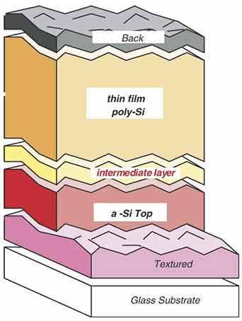 Amorphous material is used in solar cells. Single crystal silicon is the most commonly used type of silicon, as it produces the most efficient solar cells. While monocrystalline silicon can be sliced into small squares, it has a more complex structure. As such, polycrystalline silicon wafers are more efficient than monocrystalline silicon.
Wire-sawing block-cast silicon ingots make polycrystalline silicon wafers into thin slices. They are lightly p-type doped, which results in an array of small, round cells. The n-type dopants are applied to the front surface, forming a p-n junction below the surface. The crystalline silicon is then annealed at high temperatures to make it suitable for solar cells.
In the photovoltaic industry, polycrystalline silicon is the feedstock for conventional solar cells. In 2006, over half of the world's polysilicon was used by PV manufacturers. However, the feedstock shortage in 2007 hampered the solar industry. In 2008, there were only twelve factories that were capable of producing solar-grade polysilicon. Monocrystalline silicon, on the other hand, is more expensive than polycrystalline silicon, and it undergoes additional recrystallization by the Czochralski method.
Single-crystal silicon (monocrystalline) is the most common type of silicon. Single-crystal silicon has no grain boundaries and a homogeneous structure. Large single crystals are rare and difficult to produce in the laboratory. Amorphous silicon, on the other hand, is amorphous. It lacks order on the atomic level. It has a random structure and is highly conductive when formed.
Single-crystal silicon wafers are more expensive and difficult to process. But these polycrystalline silicon wafers can be fabricated into a variety of shapes and sizes. They can be used as gate electrode material for MOS devices. And because they have a very high electrical conductivity, they are an important part of photovoltaic technology. But what are Polycrystalline Silicon Wafers? You'll be pleasantly surprised to find that they are both inexpensive and versatile.
Monocrystalline silicon is the most common type of silicon. It is a single-crystal material. In nature, it is a homogenous, single-crystalline material with no grain boundaries. In the lab, it's extremely difficult to make single-crystal silicon. The amorphous form is highly disordered and has no structure at all. As a result, it is hard to produce.
The main difference between monocrystalline and polycrystalline silicon is in the amount of silicon. For example, Poly-Si is made of small grains of monocrystalline silicon. It is highly uniform and is cheaper than monocrystalline silicon. It is a very important component of solar cells. It is used in most electronic devices in the world, including solar panels, semiconductors, and transistors. When the latter are used, they are nearly identical to those made with monocrystalline silicon.
Polycrystalline silicon wafers are made of small grains of monocrystalline silicon. Monocrystalline silicon wafers are used in photovoltaic cells, while polycrystalline silicon is used for solar energy. Metallurgical silicon is fine for making metal alloys, but it is not graded for use in electrical components. It is used for a wide range of purposes, including high-tech gadgets, and can be reused.
Polycrystalline silicon wafers are the most common form of solar PV materials. They are the most popular type of solar PV material and are crucial to the manufacturing process. It can be used in a variety of different applications, and it has many uses. Its purity makes it an important component of photovoltaic technology. It can be found in a variety of applications. It is also used in other forms, such as solar modules.
What are Advantages do Polycrystalline Silicon Have?
The main advantage of Polycrystalline Silicon is its lower cost. Compared to Monocrystalline Silicon, Polycrystalline Silicon is easier to produce and is significantly less expensive. In addition, its durability is comparable to that of a monocrystalline module. Despite the disadvantages, Polycrystalline Solar Cells are a low-cost way to create a solar photovoltaic system. The low price of Polycrystalline Silicon could make solar power more affordable for those who do not have access to monocrystalline silicon cells.
One of the most important advantages of Polycrystalline Silicon is its high purity. It is the cheapest source of silicon on the market, which is why it is the most common and widely used. It is also the most popular material for solar PV due to its low cost. It is essential for photovoltaic cells, and it is an  important part of photovoltaic technology. You can find polycrystalline Silicon in many different applications, from LED lights to solar panels.
The demand for Polycrystalline Silicon soared to an all-time high in the past two decades. Since 1995, semiconductor demand has doubled from 13,600 MT to 28,000 MT, and the demand for solar PV modules has tripled every 2.7 years. Today, the demand for Polycrystalline Silicon has risen to 420,000 MT. In 20 years, demand for Polycrystalline Silicon will reach the equivalent of 28,000 MT of copper.
Polycrystalline Silicon is an important material for solar panels because it can be manufactured in near-pure form. Its high purity makes it ideal for solar panels, as it can produce nearly the same amount of energy as pure single crystal silicon. Its use in this industry is far-reaching and has become vital to the global economy. For example, it is used in microwaves, radios, and watches. It is also found in all electronic devices, from small components to the controls of automobiles.
Polycrystalline Silicon is used in the manufacturing of semiconductors. It can be used as a gate electrode material in MOS devices. Metal silicides can increase the electrical conductivity of polysilicon. It can also be used as a conductor and resistor. It can also be used as an ohmic contact in shallow junctions. Its electrical conductivity is higher than single crystal silicon, but it is more expensive.
In the photovoltaic industry, Polycrystalline Silicon is the primary feedstock in conventional solar cells. It is used for the manufacturing of conventional solar cells. In 2006, over half of the polysilicon in the world was consumed by PV manufacturers. During the year 2008, the shortage of the chemical material crippled the solar industry. It is much more expensive and less efficient than monocrystalline silicon. It is also more difficult to obtain.
The rate of polysilicon deposition increases with temperature. As a result, the activation energy of polysilicon is 1.7 eV. As a result, the rate of polysilicon deposition is faster than the unreacted silane at the surface. The higher the temperature, the higher the rate of polysilicon deposition. As a result, the price of the chemical compound fell drastically in the past several years.
Single-crystal silicon, also known as monocrystalline, is the most common type of Silicon. Its homogeneous structure can be recognized by its external colouring. The material is a continuous crystal with no grain boundaries. Large single-crystals are very rare in nature and are extremely difficult to produce in the laboratory. In contrast, amorphous structures are highly disordered and have little order. Further, their atomic-scale structure is not uniform and lacks order.
While the production of polycrystalline silicon has risen dramatically in recent years, China has recently tripled its production output from 2008 levels. By 2012, China's total output is projected to reach around three hundred thousand tons. In fact, the earth's crust is made up of 26 percent of siliceous minerals containing silicon. In the past, the Earth has had limited amounts of polycrystalline silicon, but it's now a popular alternative for a wide range of applications.
Polysilicon Applications
Among its many applications in the semiconductor industry, polysilicon is a popular gate electrode material for MOS devices. By adding a metal silicide or a metal layer over the polysilicon gate, it increases its electrical conductivity. In addition to its gate electrode function, polysilicon is also a good resistor and ohmic contact in shallow junctions. The doping process can increase or decrease its electrical conductivity according to the application and the required resistance or conductivity.
 While the underlying chemical reactions for the polysilicon deposition process are relatively straightforward, the overall chemistry is complex. The reaction rate of polysilicon is often governed by the concentration of reactants and the rate at which the gas flows. In contrast, a process involving the introduction of dopants can alter the grain size and orientation of the deposited polysilicon. In addition to its efficiency, the deposition process is very cost-efficient and produces high-quality materials.
Typical properties of polysilicon are its crystalline structure. This means that it is composed of silicon grains, or crystals. The grains typically contain millions of atoms and are arranged in a periodic structure. Unlike amorphous silicon, which is not a solid, amorphous silicon has no discernible periodic structure. It can be created by adding hydrogen or by hydrodegenation. Depending on the application, amorphous silicon is easily deposited on a large surface.
When the polysilicon undergoes oxidation, it becomes a crystal. The oxidation process occurs because phosphorus is dissolved in the silicon. This is a necessary step to make the polysilicon semiconductor. However, it is important to note that the growth of polysilicon is regulated by a variety of factors. One of these factors is the degree of amorphousness. Amorphous polysilicon will have more crystalline than amorphous silicon.
The process of removing polysilicon crystals requires a high temperature. The process requires a vacuum chamber for the process to be successful. During the oxidation process, abrasives are incorporated in a special chemical called abrasive. The additives in these processes improve the surface quality of polysilicon by increasing their adhesion strength. This is a critical step for making silicon semiconductors.
What is The Size of the Polysilicon Market
The polysilicon industry has become increasingly consolidated in recent years. The top five companies in the industry will account for 73% of global production in 2020, up from 60% in 2008. This has led to a decline in local producers and an increase in polysilicon imports. Sino-American companies are the largest producer of polysilicon in the world. They are also the biggest consumers of polysilicon in the world. So, if you're looking for a high-quality product at a low price, a higher price is the answer.
The process of doping polysilicon involves using heavily-doped glass on an undoped silicon wafer. The dopants are then dissolved in the glass, which is heated to 900 or more. This process makes the polysilicon layer annealed at a high temperature. Aside from the high temperature required in the process, it also allows for the incorporation of other substances, such as boronium.
The most common method for obtaining polysilicon is through low pressure chemical vapor deposition. Unlike other types of materials, Poly-Si is inexpensive and can be obtained at relatively low levels. Some Poly-Si uses include diffusion and electrical isolation. For other applications, the polysilicon is doped after the deposition process to enhance its performance. This process is a great choice if you're looking for a highly uniform layer of polysilicon.
In addition to its benefits, polysilicon has many applications in electronics. It boosts the performance of solar cells and semiconductors. It is also used as a base material for crystalline silicon solar cells. Whether you need a small or large quantity, polysilicon will provide you with the right material for your application. The benefits of polysilicon are endless. The material can be used for a variety of different applications, and is a great alternative to conventional crystalline silicon.
Polysilicon is an excellent material for flexible screens. It can be deposited on a variety of plastic substrates. The use of epitaxial growth tools is another technique. In contrast to PECVD, sputter deposition is a relatively new technique used to deposit a-Si without melting it. The resulting film can be removed with XeF2 gas. Regardless of the method of deposition, polysilicon is an ideal material for electronics.