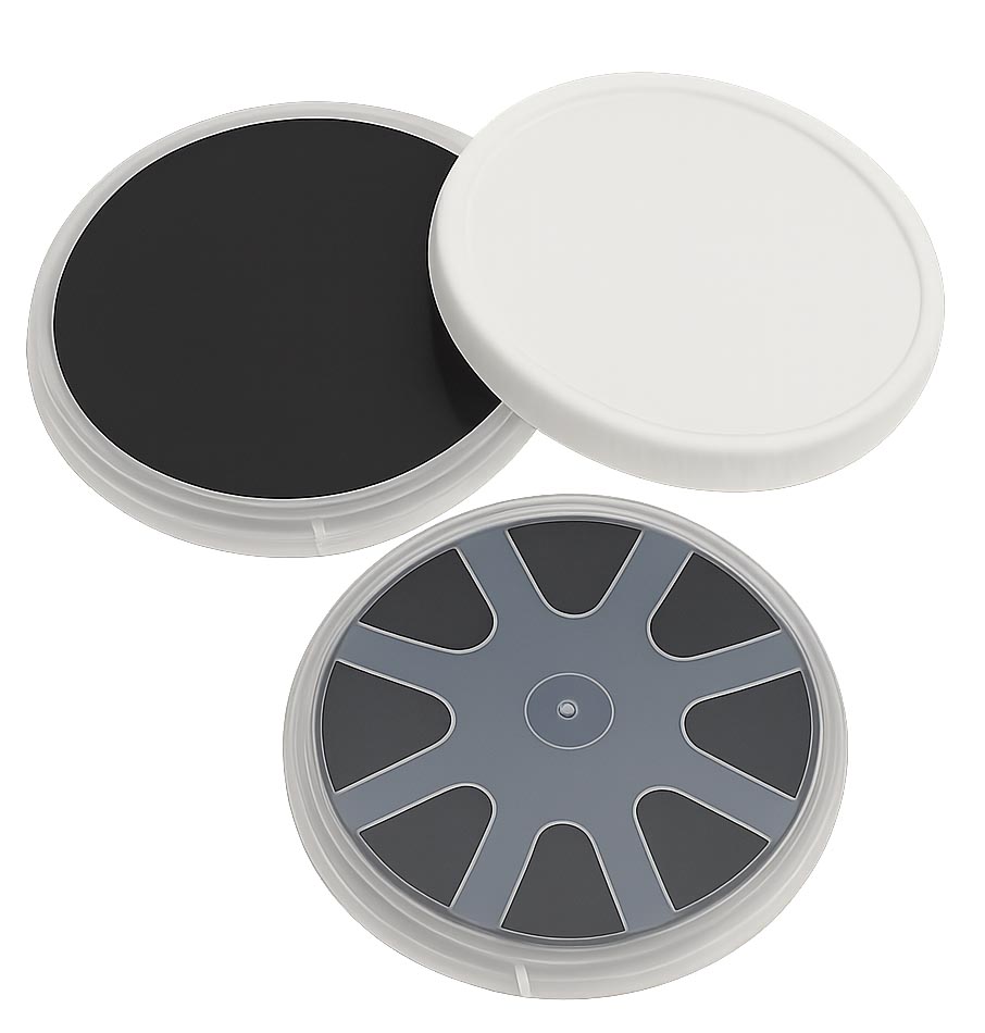
We are interested in buying InSb substrates from you.
Premium quality of the
substrates is of crucial
interest for our research
activities.
Please inform us if you can provide us with:
Material: InSb
Grade: Prime
Ori: (100)
Diameter: 2"
Thickness: 0.500 mm
Polishing: 2 sides epi polish
We would kindly like to know
what is the price for 3 pieces
of the InSb substrates with
these specifications.
Indium Antimonide (InSb) Wafers
A University Ph.D requested a quote for the following:
Please reference #221220 for pricing.
Get your InSb QUOTE FAST! Or, Buy Online and Start Researching Today!
Indium Antimonide Substrates Research
A, a leading manufacturer of indium antimony compounds, today announced that it has developed a new class of high-performance, low-cost, and ultra-thin-film substrates. The invention concerns the development of a substrate containing both indium antimony (IndiA) and antimony (Antimium) in a single atom. [Sources: 1, 7]
IndiA can be heated to temperatures of up to 1,000 degrees Celsius (3,500 degrees Fahrenheit) before evaporating, and at temperatures as high as 0.5 degrees. [Sources: 2]
The resulting indium antimonid film is transferred into a completely protective atmosphere to undergo a high temperature transfer from the surface of the film into the atmosphere and back again. On the other hand, it is very difficult to control the antimony concentration in the material and its absorption by the air. The needle - like precipitation - is distributed over the indumin and distributed as shown in FIG. Excess indium diffuses and thus an indium oxide layer is formed, which is then distributed by the IndiA film. [Sources: 4]
To understand the complex Moire patterns that appear in the TEM images, we used a combination of a calculated dislocation field and simulated diffraction contrast (Fig. 1) to construct a 3D model of a single indium antimony film with a surface of 1.5 m. To understand these complex "moire" patterns that appear on the tempos image, I used the calculated dislocation field (FIG. 2) and the simulated diffraction contrast (Fig. 3) to construct a 2D image of an IndiA film and a 1D map of its structure. To understand this complex 'Moires' pattern, which appears on a T EM-image (FIG.2), I use the calculation of calculated disOri fields (Fig.3) together with the simulated diffraction contrast. [Sources: 0]
To build the XOI platform, Javey and his colleagues built a preliminary swelling substrate and then lithographically sampled the film with an ordered series of nanobands. [Sources: 5]
Two vapors, a vacuum and an evaporator, released steam onto the substrate during rotation, and two vapor vents released steam from the evaporators onto the substrates as they spun. [Sources: 4]
Compared to pure TiO2, indium-doped boron (tio-2-aB) and tIO- 2- aIn (aA) were dosed with visible UV light and showed a significant reduction in the valence bands of both substrates. Compared to pureTiO 2, interstitial - doped B-ions hybridised in a lattice of O2P were more sensitive to the mixing valence bands formed by their hybridisation with the substrate and less sensitive to those formed from mixed valence bands by the sub-B-ion hybridisation within the lattices of T2A and T3A. In contrast, the number of Ti O 2 (sub-1, aO- sub, 2.0), Indian-dosed borson was more resistant to mixed valence band formation due to its hybridizations with Ti 2P and Ti2B and to a high degree of resistance to visible UV light from the vapour vents and evaporators. [Sources: 3]
This small QD consists of pure indium antimonids, which means that it contains no arsenic inclusions and small amounts of arsenic. This smallest QD consists of Pure indium antimones: A comparison of the properties of small qD and pure TiO 2, with and without arsenic and with a small amount of boron and tIO-2- aIn (aA). This smaller Qd consists of pure IndiaAntimones: a comparison between the properties of the smaller Qd and the purer TiO2, but with small doses of tio- 2-aB and Ti2B. This means that this small quantity has arsenic binding and a smaller quantity with or without arsenic and contains small amounts of borson. [Sources: 0]
Indium antimonids have been described by Kruse, McGlaughlin and McQnistan as semiconductor compounds produced by melting ice and stoichiometric amounts of indium and antimony. The composition of the resulting indium antimonid film is a mixture of boron and tIO-2-aIn (aIn) and a small amount of tio- 2- aB and Ti2B. A single crystal wafer, ground to a thickness of 50 Mu, is etched to give the desired pattern. Mu is obtained by controlling temperature, pressure and pressure, as well as the thickness and number of atoms in the film. [Sources: 4, 6]
The silicon in the single crystal wafer is treated with oxidative diffusion and forms a layer of silicon oxide. The indium antimonid film is then partially oxidized and crystallized again during heat treatment. During the vapor deposition process, a layer for the indium antimonides film grows on the substrate. [Sources: 4]
In contrast to conventional protective layers, such indium oxide layers have a high compatibility with the film from the Eindiumantimonide and do not decay, as shown in FIG. Therefore, it is unsatisfactory to prevent the reevaporation of antimony by applying an oxide layer to the surface of the indiamine film, but still not having the magnetic resistance of this element, which is generated by the indium antimony films. By contrast, if the indium anti-antimony oxide layer is built directly on silicon in a single crystal, it has been found to flake off during the subsequent phases of heat treatment and it has also been observed that the heat treatments associated with recrystallization are poor. Adhesion can be improved by applying a layer of India Antimonid film to a resulting substrate and then subjecting it to heat treatment. [Sources: 4]
Sources:
[0]: https://kundoc.com/pdf-structural-features-of-indium-antimonide-quantum-dots-on-the-indium-arsenide-sub.html
[1]: https://patents.google.com/patent/WO1997006555A1/en
[2]: https://www.ncbi.nlm.nih.gov/pmc/articles/PMC4805681/
[3]: https://worldwidescience.org/topicpages/i/indium+antimonide+insb.html
[4]: https://patents.justia.com/patent/5008215
[5]: https://newscenter.lbl.gov/2010/11/22/ultrathin-alternative-to-silicon/
[6]: https://www.google.sr/patents/US3554818
[7]: https://axtinc.gcs-web.com/news-releases/news-release-details/axt-announces-six-inch-diameter-indium-phosphide-substrates
Indium Antimonide (InSb) Single crystals are grown in a pure fused silica system by the Czochralski method from multiple zone refined polycrystalline ingot.
What are Indium Antimonide Wafers Used For?
Indium antimonide (InSb) is a semiconductor material that is composed of indium and antimony. It is used in the manufacture of electronic devices such as infrared detectors and sensors, as well as in high-speed electronic devices. Indium antimonide wafers are thin slices of InSb crystal that are used as the starting material for the fabrication of electronic devices. The wafers are cut from large ingots of InSb crystal using a process called wafer slicing, and are then polished to a high degree of flatness and surface finish. Indium antimonide wafers are typically a few hundred micrometers thick and are used as the substrate upon which electronic devices are built.
Scientists have used the following InSB wafer specfication to research highly-responsive Infrared (IR) photodetector sensors.
InSb Item #7400
2" Undoped [100] 500um SSP

InSb IR Sensor
InSb Electronic And Crystallographic Specifications

Raytheon's AIM-9X missile, incorporates an Indium Antimonide (InSb) bandgap detector array
InSb - Indium Antimonide Inventory
A University research assitant requested the following quote:
I am a graduate research assistant at the University of Texas at Dallas, and I am looking for price quotes on InSb and CdTe wafers for both (100) and (111) Ori. If you could give me a quote for 3" wafers, 2" wafers, and 1cm x 1cm (if available). We are not making devices with these wafers so it doesn"t matter if there is doping (cheapest substrate if fine for the price quotes).
Please reference #197392 for specs and pricing.
Undoped Indium Antimonide Wafers
Item #N797 - 2" Undoped (100) 500um SSP
N-type Tellerium (Te) Doped Indium Antimonide Wafers
Item #5138 - 2" N/Te [111A] ±0.5° 525um DSP
If you cannot use the following specs, please let us know which specs we can quote for you!
| Item | Material | Orient. | Diam (mm) |
Thck (μm) |
Surf. | Resistivity Ωcm |
Nc a/cm3 |
Mobil cm2/Vs |
EPD /cm2 |
Comment |
|---|---|---|---|---|---|---|---|---|---|---|
| N797 | undoped InSb:- | [100] | 2" | 500 | P/E | n-type | <2E14 @77ºK | >40,000 @77ºK | <300 | EJ Flats; Epi Ready |
| 5138 | n-type InSb:Te | [111A] ±0.5° | 2" | 525 | P/P | 0.0230-0.0313 | (3-8)E14 | 400,000-450,000 | <50 | 1 Flat; Epi Ready |
Indium Antimonide Substrates for THz Modulators
Scientists have used the following InSb wafers for their THz modulator research. Click here for Gallium Antimonide (GaSb) and Indium Phosphide (InP) wafer options.
| Item | Material | Orient. | Diam. | Thck(μm) | Pol | ResΩcm | Nca/cm3 | Mobilcm2/Vs | EPD/cm2 | Comment |
| 7400 | undoped InSb:- | [100] | 2" | 500 | P/E | n-type | <2E14 | US Flats; Epi Ready |
Indium Antimonide Applications
There are many different applications for Indium Antimonide in various fields. From photovoltaics to thermal imaging, indium antimonide has a wide range of uses. The article below will look at some of the more common uses for Indium antimonide. Listed below are some of the applications of Indium antimonide. We recommend that you review each application and choose the one that works best for your needs.
Infrared (IR) Detectors
Indium antimonide infrared detection is an increasingly common technology in scientific research. This material can be produced in a variety of different configurations, including photovoltaic, photoelectromagnetic, and photoconductive. Detectors based on indium antimonide have shown a wide range of sensitivity limits. In the process of making detectors, indium antimonide is doped with different levels of donor and acceptor impurities.
Due to recent advances in the semiconductor technology, InSb detectors have become more effective. They have the largest ambient-temperature electron mobility, electron drift velocity, and ballistic length of any known semiconductor material. These features make inSb a very important thermal imaging detector, which is used in many military and scientific applications. They have also been used in spectrometers and telescope sensors. However, despite their increased efficiency, indium antimonide infrared detectors are still not suitable for applications requiring a broad spectrum of wavelengths.
Indium antimonide is a crystalline compound of the elements indium and antimony. It is a narrow-gap semiconductor and is sensitive to wavelengths between one micron and five microns. It was previously used in mechanically-scanned thermal imaging systems. Today, indium antimonide is also used in terahertz thermal imaging systems. Because it is so sensitive, it is essential to obtain high-purity InSb materials for high-precision detection.
The indium antimonide photodetectors use a unique semiconductor, Indium antimonide, which has a narrow bandgap. At room temperature, InSb photodetectors can be quite sensitive, but their fragile nature makes them less flexible. Using an array of InSb nanowires on a flexible substrate can improve their performance and flexibility. Using gold nanoclusters as seeding particles, these stoichimetric InSb nanowires were synthesized using a vapor-liquid-solid (VLS) technique.
Microelectronics
Indium antimonide is a semiconductor used in a wide range of microelectronic devices. Its intrinsic properties make it ideal for a variety of applications in a wide variety of fields, including microelectronic devices. Indium antimonide is widely used in infrared detectors, airborne navigation systems, and precision targeting systems. This metal also has a wide range of applications in the field of marine infrared detectors.
Most microelectronic devices today use semiconductors as their key components. It is used in solar cells and in microelectronics. The metal's name derives from the Latin word indicum, which means violet. Because of its excellent semiconductor properties, Indium is easily grown under vacuum conditions. Its high ballistic length and low electron mobility make it an ideal choice for use in electronics.
The indium antimonide film grown in Russia is 75 mm in diameter. This semiconductor crystal is also an ideal element base in optoelectronics. It is used in the fabrication of linear photodetectors in the 3-5 mm range. Its crystals are also useful as heat vision material. They are becoming increasingly more common in microelectronics. But it is not just semiconductors.
The band gap of indium antimonide is narrow, enabling it to function in field-effect transistors. The device can be made of high-speed transistors with low power consumption. Its high-quality structural properties also make it an ideal material for digital devices. Currently, indium antimonide nanowires are being developed inside regular pores in anodic aluminum oxide. These nanowires can even be used to fabricate THz-range electromagnetic generators.
Optoelectronics
Indium antimonide is a direct bandgap semiconductor with the lowest band gap temperature, which is 300 K. It also has the largest bulk electron mobility, making it a promising candidate for high-speed and low-power electronic applications. While indium has a lot of advantages over its counterparts, it is difficult to dope the material during the electrodeposition process, so the use of other elements is preferred. Indium antimonide nanowires can be tuned by varying their aluminum concentration.
For instance, large infrared imaging sensors require high resolution and wide fields of view. In addition, the infrared detector must be cooled quickly to remove mechanical stress due to the different coefficients of expansion between the two materials. Indium antimonide detector elements form islands on a silicon substrate, and the resulting device has a near-perfect match with a silicon read-out circuit.
GaAs and InAs are two low-dimensional semiconductors that can be used in a variety of optical devices. GaAs is a common semiconductor material, and InAs can be used in QW diodes. However, the latter material can be used for optical modulation and a variety of other applications. These materials are also a viable alternative to silicon for some applications. And despite their low-reflection state, they are ideal for low-cost, small-volume manufacturing.
Indium antimonide has many advantages over silicon in optical electronics. Its narrow band gap, large Lande g-factor, and low-emissivity make it a promising candidate for many optical electronic applications. It also exhibits strong thermal conductivity. However, this material can also be expensive, so it is not a good choice for high-volume production. However, if the cost is an issue, Indium antimonide can be used for lasers as a very low-cost alternative to silicon-based devices.
Photovoltaics
Gallium antimonide, or InSb, is an alternative semiconductor material that can be used in photovoltaics. Its unique optical properties make it the ideal material for high-performance solar cells. While InSb is used for high-voltage applications, it also has several applications in other industries, including solar cells, photovoltaics, and infrared sensors. This report focuses on the latest trends and growth prospects in the global market.
The present invention focuses on the responsiveness of an indium antimonide photovoltaic detector when illuminated by an electric field with a variable absorber thickness. The device architecture is shown in Fig. 1, which represents a simulation of the device. The curve of photoresponse rate shows the responsiveness of a medium wave photodiode sample to varying illumination. The sample is also tested for its responsiveness at liquid nitrogen temperatures.
Indium antimonide is a popular choice in photovoltaics due to its high conversion efficiency and excellent optical properties. It is an excellent semiconductor and is easy to grow in a vacuum. TPV systems made of this material have an optimal emitter temperature in the range of 750-850K. The use of a photonic crystal filter increases conversion efficiency by around 2%. If the absorbing layer is too thick, the photovoltaic device fails to function properly.
Researchers at Berkeley Lab discovered that the bandgap of indium antimonide, a type of semiconductor material, is not two electron volts, as previously thought, but close to 0.7 electron volts. The bandgap of indium alloys has long been known, but their photoelectronic properties have not been fully understood. The use of indium antimonide as a photovoltaic material may help make the semiconductor technology more durable and reliable.
Solar cells
Indium antimonide solar cells are semiconductor devices that improve the absorption of light. The semiconductor material works well in the infrared region of the solar spectrum, which contains the most amount of energy for harvesting. But the efficiency of the solar cell can be decreased by removing this layer, or by using a concentrator. To understand how an indium antimonide solar cell can be improved, let's look at the different ways it can be improved.
The surface structure and internal degradation processes of a solar cell can have a significant impact on the efficiency. Compared to indium tin oxide (InP) cells, indium antimonide solar cells have an overall efficiency of 18.9 percent, and this may be a good thing. But if you want to make more efficient solar cells, you have to refine the process. A supercontinuous laser with 188 mW was used to irradiate the solar cell over a period of 67 days. The degradation was not linear, but a slight increase in efficiency was observed after 42 days. This increase is probably caused by the presence of deep donor level centers in the solar cell.
The radiation tolerance of indium phosphide is the most significant advantage compared to silicon and GaAs solar cells. The efficiencies of heteroepitaxial indium phosphide solar cells can be improved to near theoretical levels. In order to improve the efficiency of indium phosphide solar cells, researchers must improve the development of thin films. The optimal design study described here is for a high efficiency indium phosphide solar cell for space power applications. The results were evaluated by applying a PC-1D computer program.
