Looking for possibly more of these silicon wafers: Item #478. We use them as sputtering process witness coupons and really are just looking for the most affordable option we can make small coupons from. If you have other recommendations that would be great. Looking to quote or price out 250 of them.
Sputtered Films for Research & Production
Witness Coupons for Sputtering Process
A manufacturing manager requested a quote for the following.
Reference #321571 for specs and pricing.
Sputtering Service
Below you get an idea of how we help researchers with their needs.
Please quote the prices for sputtering targets as mentioned below. Sputtering Targets 75x3mm SmCo5, 99.9% Quantity required 1 pcs.
Reference #271390 for pricing
Get Your Quote FAST! Or, Buy Online and Start Researching Today!
What Are Sputtered Films?
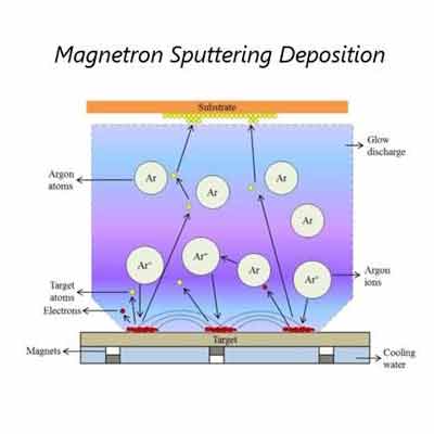
Sputtered films are thin films that are deposited onto a substrate using a process called sputter deposition. In this process, a target material, typically a metal or an alloy, is bombarded with high-energy ions, typically argon ions, which cause atoms from the target material to be ejected and deposited onto a substrate. The substrate is typically a solid material, such as a wafer, a glass slide, or a foil.
Sputtered films are used in a variety of applications, including microelectronic devices, optics, and coatings. They are highly uniform and have excellent physical, chemical, and electrical properties, making them suitable for use in a range of applications.
There are several types of sputtered films, including metallic films, dielectric films, and composite films. Metallic films are made of metals or alloys and are used as conductive or reflective layers in microelectronic devices and optics. Dielectric films are made of non-conductive materials and are used as insulating layers in microelectronic devices and as protective coatings in optics. Composite films are made of multiple layers of different materials and are used to achieve specific properties or functions, such as high reflectivity or low refractive index.
Sputter deposition is a versatile and reliable method for producing thin films and is used in a wide range of industries, including electronics, optics, automotive, and aerospace. It is particularly useful for producing high-quality, high-precision films with excellent uniformity and reproducibility.
What Are Sputtered Films Used For?
Sputtered films are a special type of thin film that is produced by a sputtering  process. These films are used in a variety of applications, including photovoltaics, solar cells, and fuel cells. These films are made by heating a target material, such as Molybdenum (Mo), to a high temperature, and then quenching the metal. The result is a thin film that is highly resistant to corrosion and other environmental hazards.
Copper (Cu) thin films
Copper is a metal at the heart of the electronics industry, and it has many important physical properties. Its conductivity is particularly good, which makes it useful in electronic devices. However, it can also be susceptible to corrosion and unwanted oxidation. A solution for this problem is the use of oxidation-resistant Cu. This could lead to a reduction in electrical consumption, and prolong the lifespan of nanocircuitry.
Several studies have examined Cu thin films. Some have used AFM to study the  surface topography of the films. Others used X-ray reflectivity measurements. Still others studied the mechanical properties of the films.
A study published in the Nature journal looked at a number of different factors. It showed that a single crystal Cu (111) film exhibited the highest resistivity, and that the largest Young's modulus came from a direct current plated copper film. It was also found that a pulsed plated copper film had the highest elongation. The most interesting part of this study was the discovery of a single-crystal Cu (111) target that can be used for sputter deposition. The result was a Cu thin film that was oxidation-resistant, which is an important property for a metal used in electronics.
Another study investigated the effect of annealing on the thin film. The results suggested that the optimal film resistivity was slightly less than that of bulk Cu. A number of other films were found to have values as high as 30 mO cm.
Various techniques were also used to study the oxidation process of Cu. These included XPS, XRR, and AFM. The results showed that the O 1s peak is not present below 250 degC, but it is present at 150 degC. Moreover, it does not disappear after a few hundred seconds of etching. It is likely that the O 1s peak is the result of diffusion of a gas-like sputtered species with a high kinetic energy. This gas-like sputtered species is believed to be a precursor to metallic Cu.
A study by Parag Gadkari also looked at the effect of annealing on the films. The results showed that a slight vertical shift in the sheet resistance was observed on the heating line. This could be the result of the formation of an oxide layer on the Cu surface above 140 degC.
Molybdenum (Mo) thin films
Molybdenum (Mo) thin films are used as electrode layers in various electronic devices. They are commonly used as back contact materials for solar cells. They can also be applied as electrodes for carbon nanotube channel transistors. Moreover, Mo films can be utilized in touch sensors. In addition, they are found to exhibit reduced resistivity.
Several sputtering parameters are used to prepare Mo thin films. They include substrate temperature, deposition power and annealing temperature. Increasing the substrate and annealing temperatures enhances the surface mobility of sputtered particles and facilitates their growth. The increased surface mobility increases the diffusibility and leads to better crystallinity. The increased temperature also helps in filling vacancies, improving the reflectance and enhancing surface migration.
Higher deposition power is also found to improve the surface morphology of sputtered films. The increased deposition power reduces the microstrain and increases the film thickness. It is therefore important to measure the thickness of the films. This measurement is done using a Bruker Dektak stylus profiler. The thickness is then analyzed by measuring the average step height, root mean square roughness and surface kurtosis.
The grain size of the Mo thin film is also a major factor that affects the conductivity. The larger the grain size, the lower the inclusion of impurities and the fewer voids. In addition, the greater the grain size, the better the crystallinity of the film. The smallest resistivity was observed in the film annealed at 400 degC.
To determine the conductivity of the Mo/Cr bilayer films, different deposition powers and annealing temperatures were applied. The results showed that the conductivity ranges between 0.9 and 1.2 mm. The highest conductivity is achieved at 100 W. This deposition rate is 0.22 nm/s after 20 minutes of deposition.
During the process of analyzing the grain structure of the Mo thin film, atomic force microscopy (AFM) was employed. The image analysis program P9 is then used to perform quantitative information on the individual grains. The results show that the grain size of the film varies from 11.7 to 48.5 nm. The NT-MDT Solver-Pro atomic force microscope is also used to characterize the surface texture of the Mo thin film.
Chromium (Cr) on a molybdenum target
Chromium (Cr) is a heavy metal with various industrial applications. It is widely used in electroplating cleaning agents, as well as in the manufacture of chromium-containing compounds. It is a hard, brittle, and corrosion-resistant metal. The metal is commonly found in the trivalent Cr(III) form, but hexavalent Cr(VI) is also available.
Although chromium has many beneficial properties, it has also been shown to cause immunosuppression and cancer. Chromium enters the body through the skin, the lungs, and the gastro-intestinal tract. It is excreted through the kidneys. During the process of detoxification, chromium combines with free oxidizing radicals to form reactive oxygen species, which in turn damage membranes and tissue. The result of this reaction is apoptosis and hypersensitivity.
Studies have shown that chromium exposure can trigger apoptosis in human lymphocytes. In addition, chromium induced oxidative stress leads to lipid peroxidation, oxidative deterioration of proteins, and genomic DNA lesions. This process also results in a cascade of cellular events, including the modulation of the apoptosis regulatory gene, p53.
The bioavailability of chromium determines its biological effect. Occupational exposure involves handling cement and tanning leather, while non-occupational exposure occurs through ingestion of chromium-containing foods.
Chromium is an irritant in contact with the skin and bronchial airways. The metal is toxic to macrophages and can suppress the immune system. It is a known cause of lung cancer. It is thought to be involved in two types of hypersensitivity reactions, namely type I and type II.
The toxicity of chromium is attributed to its interaction with cellular ligands. Binding to these ligands may play a role in genotoxicity. The resulting chemical complexes may be metabolized into reactive intermediates that contribute to oxidative stress and apoptosis.
Some epidemiological studies have reported conflicting results for cytogenetic effects of chromium on lymphocytes. While some have found no significant cytogenetic changes, others report increased cytogenetic activity. In addition, Cr-induced apoptosis has been shown in human lung fibroblasts.
As a result, chromium is regarded as a potential pollutant. It is commonly used in the production of industrial chemicals and in the metalworking industry.
Quasi-reactive sputtering
Reactive sputtering is used for the deposition of thin metal films on substrates. The process involves the surface of the target being bombarded by argon ions. This allows for high control over the composition of the deposited film. It also ensures that the film adheres to the substrate.
The sputtering process is governed by mass-balance equations. The reactive gas flow is plotted against the chamber pressure and the deposition rate. The deposition rate is then related to the power consumed per magnetron length and the normalized dynamic deposition rate.
The energy of the species striking the growing film affects the density and the columnar morphology. It also determines the residual film stress.
Reactive sputtering is used to create low-temperature, low-growth films that are suited for applications such as ferroelectrics and oxide thin films. The method is a combination of sputter deposition and PECVD. The technique was initially applied to tantalum nitride resistors.
Reactive sputtering provides a high degree of control over the stoichiometry of the deposited film. This can be done by modifying the composition of the reactive gas. For example, a reactive gas might be nitrogen, which is often used to modify the composition of titanium nitride.
Besides reactive sputtering, other methods of sputtering include RF diodes and planar diode discharge devices. These are used for plasma-assisted etching and PACVD. These techniques have been applied to a number of different materials.
The sputtering process can be simulated using computer simulation. This can be useful in determining the effect of reactive gas pressure, flow and the sputtering rate. It can also be used to analyze the transport of the sputtered material from the target to the substrate.
For the study, a number of experimental setups were used. All were investigated for their effects on lifetime. The setups were tested with a single-tube (A1) or a double-tube (A2) configuration. For the A1 setup, iVoc was lower, which leads to lower lifetimes. On the other hand, the double-tube configuration resulted in higher lifetimes, which were attributed to a decrease in iVoc.
Video: Learn about sputtered thin films
