I would like to obtain a gallium arsenide wafer with diameter preferably around 4 inches (though other sizes are acceptable) for use in academic research in materials science in this university. Would it be possible for you to send me a sample piece? The specifications are very flexible.
What is the Dielectric Behavior of Substrates?
What Wafers Do I Use for Researching Dielectric Behaviour?
A university materials scientistist requested a substrate for academic research dielectric behaviour of Gallium Arsenide wafers (GaAs).
Please reference #270690 for specs/pricing.
Get Your Quote FAST!
What is Silicon's Dielectric Constant?
Silicon's dielectric constant is about 11.7, but differs depending on the type of silicon and the fabrication process used to make it. The dielectric constant of silicon is an important parameter when designing semiconductor devices, because it influences both capacitance and the signal propagation within a device.
A large semiconductor company requested the following:
Please quote your lowest price for the following:
Silicon wafer with copper coating specs as below,
Quantity: Minimum Order Quantity
4” silicon wafer, with the below Specs
- Copper Coated Silicon Wafer (Single Side coating)
- Wafer Thickness- 0.4mm and 0.8 mm
- Copper coating thickness- 35 micron (or whatever is available readily in stock)
- Silicon Dielectric Constant- 11.9
- Lossless substrate
Reference #236843 for specs and pricing.
What is Dielectric Behavior?
When you're talking about dielectrics, you're describing the properties of an electrical insulator that can be affected by an applied electric field. In other words, dielectrics can become polarized. If you apply an electric field to a dielectric, it can either become polarised or remain neutral.

Paraelectricity
Paraelectricity is a property of a material that exhibits polarization enhancement due to a change in the electric field. Paraelectric materials exhibit enhanced nonlinear polarization compared to linear dielectrics. In addition, the electric permittivity of these materials is not constant, but varies with the applied electric field.
In general, most dielectric materials exhibit paraelectricity. However, some materials exhibit the opposite. For instance, lithium niobate is ferroelectric at low temperatures but transforms into a disordered paraelectric phase above that temperature. This behavior is also observed in some perovskites. In some cases, paraelectric materials can be used in heat pumps, in which the negative capacitance is used to operate the device.
Paraelectricity in dielectric behavior occurs when the real and imaginary parts of a complex dielectric function have different contributions to the polarization. This polarization is characterized by the polarization of electrons and ions, which is observed only at low frequencies. The electric dipole contribution is typically visible up to a few gigahertz. The two kinds of polarization can be distinguished because of the differences in temperature dependencies.
Paraelectricity in dielectric behavior is observed in many ferroelectric materials, including magnets. In these materials, the electric permittivity varies as a function of an external electric field. In addition, the slope of the polarization curve changes with changes in the electric field. Ferroelectric materials exhibit a peculiar polarization curve that shows a hysteresis loop. The direction and magnitude of the applied electric field determine the direction of spontaneous polarization.
Atomic polarization
Atomic polarization is a common phenomenon in all polymers. Unlike orientational polarization, which is instantaneous, atomic polarization is a process that follows an oscillating electric field. However, it contributes less to the overall permittivity of the material than does electronic polarization.
An atom has two polarization states: positive and negative. A positive charge will reside on the surface, and a negative charge will reside on the opposite surface. The net charge is equal to the sum of the positive and negative charges. The dielectric constant is 4.5. This constant enables us to calculate the electrical field on a dielectric material.
The Stern layer, also known as the 'Stein layer,' is formed by two processes. First, it is affected by the presence of ions, such as zinc, which is an element that can have a large impact on the phase angle of induced polarization. Second, the Stern layer affects the frequency-dependent electrical flow in saturated rocks.
Dielectric material has a large electric field due to the presence of the ion titanium. The titanium ions in barium titanate have high ionic polarization. As the temperature increases, they move from one direction to the other. The cubic lattice, however, resists large motions, and so the titanium ions jam up on the crystal cell, leaving it with a permanent dipole moment.
Atomic susceptibility
Atomic susceptibility to dielectric behavior is a property that describes how well a material can conduct an electric current. It is a measurement that is important to engineers, scientists, and biomedical researchers. This property, also known as the dielectric constant, is a dimensionless quantity that can vary from material to material. The frequency at which it changes is an important factor in determining the susceptibility of a material.
The temperature dependence of dielectric properties has several implications. For instance, in an electric current, a high temperature will cause the dielectric constant to decrease. At low temperatures, this means that a material will not be as sensitive as another. Atomic susceptibility to dielectric behavior is important because it can provide important information about the water content of a material.
A recent study has uncovered a tunable peak in the (n) dielectric spectrum that is centered at about 20 GHz. This Debye peak indicates that collective dipole moment relaxation is occurring on a timescale of 8.3 ps. A similar peak in O has also been found in both coherent and incoherent neutron scattering experiments.
Dielectric constants of two-dimensional materials can be rescaled to account for different thicknesses. For example, the dielectric constant of monolayer MoTe2 approaches vacuum when interlayer separation is infinite.
Atomic permittivity
Atomic permittivity and dielectric behavior are properties of materials that can control electrical current. This is achieved by determining the dielectric constant of a material. Dielectrics have dielectric constants greater than 1, and their conductivity is low. The constant of dielectrics is defined in Table 2.
Atoms with large electron clouds are expected to have high polarisability. The higher their polarization, the higher their dielectric constant. Fluorine, on the other hand, is a low-polarisable atom due to its small radius and concentrated negative charge. As a result, fluorine's dielectric constant will be lower.
Atomic permittivity and dielectric behavior can be described by a two-phase model that takes into account the contribution from different sources. These sources can be dipolar, space charge, or ionic. Each of these factors contribute to the overall dielectric response. The two-phase model also accounts for the influence of microstructure on relative permittivity. For example, in ferroelectric materials, the dipolar contribution is the largest contributor.
The charge distribution of Si atoms is very narrow, with an average charge value around -0.85. The oxygen atoms, on the other hand, have no effect on the dielectric constant and are polar at high Zr contents. The shift toward higher and lower charges induces a larger heterogeneity in the local charge distribution, which may increase the dipole moment fluctuations and the static dielectric constant.
Atomic polarization tensor
The atomic polarization tensor of di electric behavior (APTD) is the tensor of a crystal's polarization. It is calculated by performing coupled perturbed Kohn-Sham calculations of the dielectric constants e and n. It is useful for evaluating the anisotropy of a crystal's optical indicatrix.
Its physical dimension is C/m2 (coulomb per square meter). In addition, a material's polarization has a vector dimension (P). The sum of all dipole moments has an area charge of zero. Therefore, a material's polarization is non-uniform.
The atomic polarization tensor depends on the electric field at earlier times. When applied with a strong electric field, the electric field causes the dipoles to align in the direction of the field. If the electric field is removed, the dipoles' polarisation returns to zero.
Induced polarization in solids is an important characteristic of porous rocks. Since oil and gas have lower dielectric constants than water, measuring their dielectric properties is a useful way to monitor the relative levels of hydrocarbons in geomaterials. Vanhala (1997) used induced polarization to map oil-contaminated till and sand.
Atomic polarization loop
Atomic polarization is the process in which an atom's electrons are polarized. This polarization is a characteristic of all cells, including those of living organisms, to some extent. It results from the complex interplay between ion transporters and ion channels. Different parts of the cell have different ion channels and electrical properties, which can affect their polarization.
An electric field can cause an atom to polarize, and the polarisation depends on the previous electric field. A power law explains this behaviour, which can be represented by an integral over weighted exponential functions. As the dielectric constant is 4.5, the polarisation of an atom is determined by its dielectric constant (Khe(o)).
An electrical field varies with temperature, but the magnitude of the change is not directly related to the temperature. However, the hysteresis loop varies with temperature. The lower the temperature, the less thermal motion is present, and the higher the temperature, the larger the hysteresis loop will be.
The electric field in a large piece of dielectric is equal to the electric displacement in a small spherical cavity. Then, the applied field changes its value in terms of the induced dipole moment. This dielectric moment is parallel to the direction of the electric field E.
Video: What are Dielecrtric Materials?
Silicon Dielectric Behavior
Permittivity
Permittivity is a property that describes a material's electrical behavior. It is measured in farads per square 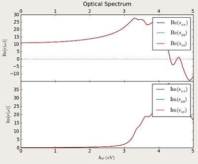 meter (F/m2) and is related to the electric field, which describes the interaction between charged particles. A material's permittivity depends on two important properties: the electric field and the density of charge.
Permittivity is an important property to understand because it determines how fast or slow a substance conducts electricity. It also relates to its temperature. For example, a material with a high permittivity will conduct electricity faster than one with a low permittivity.
The dielectric permittivity of porous silicon describes the polarization of atoms and impurities within the material. Below one hundred Hz, the material's dielectric permittivity decreases, and at higher frequencies, the permittivity remains constant. The dielectric permittivity of silicon remains constant up to one hundred kHz.
Complex permittivity relates the properties of materials in terms of their real and imaginary components. The real part of the permittivity, e, has zero or infinite conductivity, while the imaginary part is negative. Those with a low real permittivity are called lossless media.
To measure the dielectric permittivity of silicon, we performed a series of electrical measurements using small parallel-plate condensers. We found that silicon and germanium had similar permittivity, with the difference in dielectric constant being only a few percent. However, the two metals have slightly different dielectric constants, averaging around 11.7+0.2 and 15.8+0.2, respectively.
At high frequencies, phonon absorption becomes dominant. This makes resistivity less important. However, at microwave frequencies, resistivity becomes important.
Dielectric loss tangent
The Dielectric loss tangent in silicon is a property that can be measured with high precision. It shows the frequency dependence of dielectric loss and its tendency to decrease with frequency. It can be measured with the same accuracy as the Q-factor. The TEo mode is defined as a combination of the radial and axial modes.
In the microwave band, the dielectric loss tangent is mostly imposed by phonon absorption. At high frequencies, the importance of resistivity diminishes, and the absorption of free charge carriers takes over. This property makes it possible to improve the performance of silicon at microwave frequencies.
The Dielectric loss tangent in silicon is equal to 1.2 x 100 - 5 at microwave frequencies. Its value varies depending on the process used to make the semiconductor. The dielectric constant is a measure of its lossiness, and it can be very high or low depending on how it is manufactured.
The loss tangent follows a similar pattern as the loss factor and has maximum values at temperatures around 200 and 250 degC. This property is a key factor in determining the sensitivity of silicon to electrical signals. This property is also important for the production of semiconductor devices. However, the magnitude of the loss tangent has to be considered carefully.
HR-Si
The dielectric permittivity of porous Si is the characteristic property that describes the polarization of atoms and impurities inside the material. At low frequencies, it is constant; while at high frequencies, the dielectric permittivity decreases slightly. The dielectric permittivity of porous silicon is determined by two factors: the morphology and the structure of the material.
In this study, researchers found that the dielectric properties of a 150-mm-thick PSi layer with 76% porosity were nearly constant over the frequency range from 140 to 210 GHz. Broadband electrical measurements were combined with electromagnetic simulations to find that the dielectric permittivity and loss tangent are nearly constant at the frequencies studied. In addition, the dielectric properties of CPW TLines and quartz were compared.
High-purity silicon exhibits dielectric properties that are practically non-dispersive and exhibit very low dielectric loss. The dielectric loss tangent is 1.2x10⁻⁵. Such properties make silicon an excellent choice for use in microwave and radio frequency applications. However, it is essential to understand the physics behind the dielectric properties of silicon to improve its performance.
High-quality RF performance of HR-Si devices is achieved mainly by improving the effective substrate resistivity. Higher effective substrate resistivity results in lower attenuation losses and reduced non-linearities, and improves the quality factor of transmission lines and inductors. In addition, porous Si has a low cost and CMOS compatibility.
The HR-Si dielectric behavior is a function of the band-width of the crystal structure. The second lowest VHS structure in flat silicene results from a (pi) band minimum at the (Gamma) and a sigma-3) band maximum at the M position.
PSi
Silicon dielectric behavior can be characterized using several techniques. The dielectric permittivity of porous Si is a measurable property that describes the polarization of atoms and impurities within the material. For frequencies below 100 Hz, the permittivity is almost constant, while at higher frequencies the dielectric permittivity decreases. The loss tangent is the relationship between the dielectric permittivity and the frequency.
The dielectric property of a material depends on its morphology and structure. The dielectric properties of a material can be determined by different methods, including experiments. Some of these methods include a combination of simulation and measurement. This approach is useful in determining the dielectric behavior of a material.
The dielectric constant of silicone is 0.43 eV. Its loss factor increases with temperature. The loss factor is dominated by hopping charge transport and dc conduction. Silicon is also a good material for high voltage insulation. The Havriliak-Negami model accurately characterizes the dielectric properties of silica filled silicone rubber.
The stability of dielectric properties is important for high-voltage and electronic applications. The resistivity of a film may be temperature dependent using the Arrhenius equation, and the slopes of the logarithmic resistivities versus temperature are equal to the activation energy of the material. Nanocomposites of silicon dioxide and silicon rubber show less temperature dependence than their silicon counterparts.
A semiconductor calculator is a handy tool for determining the conductivity, mobility, and concentration of a semiconductor material. The calculator also allows you to compare low and high dopant densities.
Video: Dielectric Properties
What is the Dielectric Behavior Gallium Arsenide?
Gallium arsenide (GaAs) is a semiconductor with remarkable dielectric behavior. This material is very important  for understanding molecular interactions and structural changes. In this article, we will discuss some of the important properties of GaAs. Also, we will discuss the Brillouin zone and Exiton energy spectrum.
Exiton energy spectrum
The exciton energy spectrum of gallium arsenite has been studied using photoluminescence and reflection. These techniques were used to probe the spectral shape of the gallium arsenide bandgap. This study reveals that the band gap energy is about 1.5195 eV.
Point defects
The dielectric behavior of GaAs diodes is influenced by point defects in the structure. The presence of AsGa or AlAs antisite defects leads to a quasi-dielectric state. Similarly, AsAl or GaAs antisite defects exhibit a higher formation energy. The interstitial phase stability follows a Gaint-Alint-Asint pattern, with AsGa and AlAs defects being preferable in the GaAs/AlAs SL structure.
While the energy content of a single ideal split interstitial is not known for gallium arsenide, it has been reported that a single defect in Fe can contain two or more SIAs. An ideal split interstitial is actually an energy released during the relaxed formation process. Point defects are crystalline defects associated with one or more atomic sites. They can be self-interstitials or vacancies. The latter are spaces in the crystal that should be empty. In addition, they are associated with dispersed impurity atoms.
Various models have been proposed to explain the different types of defects in gallium arsenide. Density functional theory has been used in the study of these defects. First-principles models have been developed for both isolated defects and ternary complex defects. They can be used in the development of new materials and in understanding their behavior.
Point defects in gallium arsenide have different effects on the dielectric behavior. The AsX antisite defect induces metallicity, while the XAs defect exhibits spin splitting.
Thermal conductivity
Thermal conductivity of gallium arsenides is studied at a wide range of temperatures. This work compares the thermal conductivity of single crystals with data from a crystalline tellurium-doped gallium arsenide. At low temperatures, the tellurium-doped gallium acsenide exhibits a behavior similar to that of a standard gallium acsenide.
The thermal conductivity of gallium arsenide can be measured as a function of its bulk resistivity. This material's bulk resistivity ranges from 10-3 ohm cm to 108 ohm cm, a value about six orders of magnitude higher than that of silicon. The high resistivity allows GaAs to be used in a variety of electronic applications, including high-speed sensors, high-power amplifiers, and high-frequency circuitry. Despite its high resistivity, the material is not suitable for quantum well devices. In addition, silicon has several major advantages over GaAs in integrated circuit manufacturing. These include its abundant supply and low processing costs.
Thermal conductivity of gallium arsenate is measured in the kBa-As range. GaAs has a high temperature coefficient, but it is still below the limits set by other semiconductors. It is also subject to hot phonon effects, which can affect GaAs-based devices.
The band gap of GaAs depends on the temperature and the semiconductor material. It is 1.42 eV for undoped GaAs. Its electron affinity, measured as energy required to remove an electron from its bottom conduction band, is 4.07 eV.
Brillouin zone
We have studied the dielectric behavior of a gallium arsenide superlattice using spectroscopic ellipsometry, a rotating analyzer, and synchrotron radiation. We have used a broad spectral range, which gives us access to the excitations of Ga 3d core levels, which are located 20 eV below the conduction band minimum. The results show that the Ga 3d core level exhibits a strong atomic-like behavior.
The effective masses of GaAs are measured in units of free electron-mass, m. The m e represents the effective mass of an electron in the bottom conduction band, while the m hh and m lh represent the effective masses of light and heavy holes.
The electron velocity and mobility of gallium arsenide is higher than that of silicon, making it a desirable candidate for electronic applications. Its larger energy band gap also makes it relatively insensitive to overheating and produces less noise than silicon devices. It also has higher carrier mobilities and lower parasitics than silicon. This makes it a useful semiconductor for electronic circuitry, and is commonly used in mobile phones, satellite communications, and higher frequency radar systems.
The real part of the GaAs dielectric function is not flat, but instead increases with increasing photon energy in some regions. In these regions, there are a pair of major peaks at low photon energies. Interestingly, these peaks are redshifted.
Intensity of bandgaps
Gallium arsenide is a semiconductor material that has similar properties to silicon. However, this new material is characterized by different bandgaps and has the advantage of being able to change its bandgaps at will. Its fundamental energy gap is 1.519 eV. This means that it is more suited for semiconductor devices.
The bandgaps in gallium arsetide are characterized by different physical and electronic properties. For example, the direct bandgap in GaAs has a higher saturation electron velocity. Moreover, the dielectric constant is small and the carrier mobility is high. These properties are reflected in the thermodynamic properties of gallium arsenide.
As a result, the intensity of bandgaps in GaAs deep centers is shifted to different wavelengths depending on the excitation wavelength. For example, excitation at 808 nm yields brighter PL than that at 980 nm. The photoluminescence intensity is usually used to measure absorption. It is also important to remember that efficient absorption in this novel material occurs at only 980 nm.
The excitation process excites the carrier from the valence band to the conduction band, leaving a hole in the valence band. As the energy increases, the absorption coefficient increases steeply. The absorption coefficient is proportional to the square root of the energy of the photons. In addition, the absorption length decreases to a few micrometers above the bandgap energy. This is consistent with the Franck-Condon shift.
Temperature dependence of bandgaps
The temperature dependence of gallium arsenide band gaps has been studied using a model developed by Blakemore. This model calculates the band gap for different temperatures in the range of 0 K to 300 K. Using the data from this model, the band gap in GaAs is about 1.5 eV at 0 K and around 1.43 eV at 300 K.
The temperature dependence of gallium arsenide band gap is related to electron mobility, which is a measure of the ability of incident photons to excite an electron from the valence band into the conduction band. The higher the mobility, the faster the electron can move through the conduction band. This means that GaAs has an advantage over silicon when operating in the microwave region.
It has also been reported that e-h recombination results in an emission peak above the band gap. This is inconsistent with the ideal model, which predicts that the PL intensity drops to zero on the low energy side. The observed emission is likely a result of localized defects, disorder, or bound excitons in the material. The density of states (DOS) is described by an exponential decaying line shape.
A previous ellipsometric study revealed a linear temperature dependence of the optical band gap of gallium arsenide (GaAs) and indium phosphide (InP) semiconductors. They also showed that monolayer TMDs show a strong optical absorption at 3.0 eV. The band gap of monolayer TMDs is 2.97 eV at 4.5 K.