What Wafers are Used to Fabricate a Silicon Filter?
What Silicon Wafer is Used to Fabricate Silicon Filters?
A PhD researcher requested a quote for the following for their silicon filter research:
"200 um Si type N wafers price please What is the infrared transmission range. They should have a transmission in the mid infrared down to 11 um if possible. Polished on both sides with no dopants. I have attached an article where they ground the Si to 0.2 mm. Off-the-shelf would be better to begin with."
UniversityWafer, Inc. Quoted:
Si Item #E0128
50.8mm Undoped [100] 250um DSP FZ >20,000 ohm-cm SEMI Prime, 1Flat, MCC Lifetime>1,000μs
Reference #270676 for pricing.
Get Your Quote FAST!
What is Silicon Infrared Transmission Range?
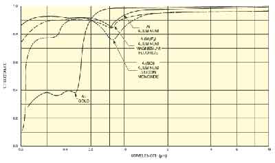
Silicon infrared transmission range is the spectral range of the material's infrared emission. This range is used in thermography and pyrometry. The transmission spectra for the materials shown in Figure 1 are nearly identical. However, they differ in the wavelength ranges. The 3-5 um range has nearly no absorption, while the 6.5-25 um range exhibits significant absorption. Thickness also influences the transmission strongly at the longer wavelengths.
The infrared region is divided into three subbands, namely, the short-wave and mid-wave infrared. The first is closest to the human eye, followed by the far-infrared. There are other definitions, including the infrared band, which follows a different physical mechanism. The sensitivity range for common silicon detectors is 1.050 nm, while InGaAs detectors have a range of 950 to 2600 nm. There are no international standards, however, for this range. In long-distance telecommunication networks, the C-band is the dominant band, while the L-band and S-band are less well established.
The infrared transmission range of silicon has been largely untapped. This is because silicon is widely used in microelectronics, and the material's optical properties are limited to the visible and partial near-infrared range. However, researchers have been able to engineer silicon nanomembranes using strain engineering to tune the material's optical bandgap. This process is now enabling silicon-based photovoltaics and image sensors.
Below are just some of the key terms associated with silicon filters.
- wavelength filters
- photon filter
- silicon photodiodes
- broadband filters
- compositional filter
- optical filter
- filtering schemes
- filters linearity
- spectral responsivity
- filter performance
- wafer help
- multipole photon
- mrr filters
- silicon wafer
- Diode responsivity
What Is a Silicon Filter?
Silicon filters are useful for a variety of applications. They are highly resistant to heat and abrasion, and have  good chemical resistance. In addition, they can handle exposure to acid and alkali. So, they are highly durable and can be used to protect sensitive electronic equipment. The next time you need a filter, consider a silicon carbide filter.
Infrared silicon filter
An infrared silicon filter can help you block out a range of wavelengths. These filters are commonly made of multiple layers of different materials. The thickness of the filter can be adjusted to match your exact needs. Typically, an infrared silicon filter will have a FWHM passband of 95 nm. If you need to block out longer wavelengths, you will need to choose a material with a higher FWHM.
There are several ways to manufacture an infrared filter. One method is by vacuum deposition, in which the bulk material is heated in a vacuum chamber until it sublimes or molten. The vapor then condenses uniformly across the surface of the optical filter substrate. The resulting layers are then built up.
Another method is to use a gas-band filter. This type of filter is used to separate the signal from the background. Because gas absorption occurs at narrow wavelengths, these filters have a narrow FWHM. This makes it possible to distinguish the gas from the background signal. Custom infrared neutral density (ND) filters are also manufactured by vacuum-depositing thin films on a germanium substrate. The goal of an ND filter is to provide linear transmission over a specific wavelength range.
Another technique for producing narrowband filters uses sputtered silicon films. This method is used to create silicon filters with high efficiencies. One of the benefits of this technique is that it can make the silicon layer narrower. This process also produces a narrower bandwidth.
Nanoporous silicon membranes
Nanoporous silicon membranes are highly porous, allowing filtration of molecules of interest with high selectivity. The pore diameters and shapes are fully controlled and can range from a few hundred to billions of pores per square centimeter. These membranes can be tailored to be highly porous or ultra-low-porosity, as required.
These ultrathin silicon-based membranes have excellent mechanical and chemical properties, and are easily manufacturable. Nanoporous silicon-based membranes can be made with silicon nitride, which has robust chemical and mechanical properties. Nanopores can be controlled by reactive ion etching. The process requires the use of a template structure and a large amount of silicon.
Several fabrication techniques are available for the fabrication of ultra-thin SiN membranes. One technique is based on ion track etching, which allows for the fabrication of conical and double-conical pores. During this process, heavy ions are accelerated to create a thin layer of silicon nitride, which is then chemically etched to create the membranes. The resulting membranes are highly porous, and can be patterned using photolithography.
Nanoporous silicon membranes are useful for a wide range of applications. They can be used for single-molecule DNA analysis and biomolecule translocation.
Thermal stability
A synthesis of inorganic-organic composite structures can improve the thermal stability of silicon filters. It can also increase their mechanical strength. These new filters are recyclable and exhibit good filtration efficiency. This research provides insight into the advantages of silicon-based filters. Further, it provides a new material for filter applications.
In this research, ultrathin a-C films were grown on silicon substrates using reactive RF sputtering. The resulting film had an underlayer of SiNx, which prevented the carbon from migrating into the silicon substrate. The resulting sub-five-nm-thick films exhibited desirable morphology. Moreover, the thermal stability of these films was determined by EELS spectra.
Using a plasmonic metal disk array (PMDA) with tantalum (Ta), the researchers fabricated thermally stable optical filters in the mid-infrared (MIR) region. The spectral response of these filters was compared to the performance of conventional silver-based PMDAs. The researchers applied the finite-difference time-domain method to analyze the effects of the geometric configuration and constituent materials on the transmission spectra. Ta-based MIR PMDAs displayed similar optical properties to Ag-based PMDAs.
The structure of silica filters varies greatly. They can be honeycomb-shaped, flat sheets, or multi-channeled. Their pore sizes and porosity depend on the precursor mixture and the sintering conditions. The composition of silica particles allows for a precise control of pore size, which enhances their desirable thermal stability.
Chemical inertness
Silicon filters are inert to most organic materials, including metals, acids, and other chemicals. They are often used in filtration processes where they remove sample contaminants or particulate matter. Silicon filters are particularly suitable for filtering grey, ductile, and non-ferrous metals because they are chemically inert and have high mechanical and thermal strength.
Silicon is a versatile material that has many uses. Its chemical inertness makes it highly resistant to acids and other aggressive chemicals. It is also non-corrosive, making it suitable for a wide variety of environments. It is also extremely durable and dimensionally stable.
Silicon is in the same group as carbon in the periodic table, but has a different chemical makeup. Silicon forms many silicides with other elements, which are useful in metallurgy. It has high hardness and chemical inertness, and resists oxidation and water. This property makes it a useful material for furnace components and bearings.
The chemical inertness of silicon filters is measured by the number of oxygens a silicon can bind. This can be easily determined by using the number of hydrogens and oxygens present in a silicon molecule. The proportion of M, T, and Q groups in a silicon molecule is variable and affects the molecule's properties.
Resistance to weathering
Resistance to weathering of silicon filters is a crucial consideration for the production of solar panels and other solar energy devices. Solar panels and solar cells are very sensitive to climate change, and therefore, it is important to maintain their performance under such conditions. Fortunately, solar panels made of silicon have excellent weathering resistance. However, it is important to note that the resistance to weathering of silicon filters varies from product to product.
The chemical weathering of silicon filters can change the minerals found in the material. Depending on the chemical conditions, the minerals may break down or dissolve in water, or they may be carried away as a hydrolysate. Water can also react with certain minerals to produce secondary minerals. For instance, the minerals feldspar and quartz often react with water to form clays. Other minerals, such as aluminum hydroxides, can also break down.
Water is the most abundant liquid in the world, and some minerals are more resistant to weathering than others. For example, quartz and certain feldspars are relatively resistant to weathering. However, many other minerals are soluble in water, and some minerals break down more easily than others.
The resistance of a silicon filter to weathering depends on the climatic, lithologic, biospheric, and pedologic settings in which it is used.