
We need silicon wafers for ALD deposition tests. The wafers do not need to be prime grade, and their electrical properties are not especially important. Undoped silicon may be preferred for optical thin-film characterization.
What Substrates Are Used for Atomic Layer Deposition?
UniversityWafer supplies a wide selection of semiconductor wafers and research substrates for atomic layer deposition (ALD), thin-film coating, surface passivation, dielectric deposition, optical characterization, MEMS fabrication, and nanotechnology research.
Common ALD substrate options include:
- Silicon wafers
- Thermal oxide-coated silicon wafers
- Silicon-on-insulator wafers
- Sapphire substrates
- Silicon carbide wafers
- Gallium arsenide wafers
- Gallium nitride substrates
- Germanium wafers
- Fused silica and glass substrates
Wafers can be selected by diameter, thickness, crystal orientation, conductivity type, resistivity, surface finish, oxide thickness, and grade. Prime-grade wafers are suitable for advanced fabrication, while test-grade, mechanical-grade, and reclaimed wafers may offer a lower-cost option for ALD process development and equipment testing.
Silicon Wafers for ALD Deposition Tests
Silicon is one of the most commonly used substrates for ALD research because it is widely available, compatible with semiconductor processing, and suitable for electrical, optical, and materials characterization.
A Ph.D. candidate requested the following silicon wafers for an atomic layer deposition project:
Reference #110676 from UniversityWafer, Inc.
Choosing Silicon Wafers for ALD Research
The best wafer specification depends on the planned coating, deposition temperature, characterization method, and final device application. Researchers may consider:
- Wafer grade: Prime, test, mechanical, or reclaimed
- Doping: Undoped, p-type, or n-type
- Resistivity: Low, standard, or high resistivity
- Surface: Single-side polished or double-side polished
- Orientation: Common options include <100> and <111>
- Surface layer: Bare silicon, native oxide, thermal oxide, or deposited films
- Diameter: Small research pieces through full-size semiconductor wafers
Undoped or high-resistivity silicon wafers may be useful when electrical conductivity could interfere with optical measurements. Test-grade or mechanical-grade wafers can also be appropriate when the goal is process optimization rather than final device fabrication.
Request ALD Substrate Pricing
Send us your required substrate material, wafer diameter, thickness, orientation, surface finish, grade, quantity, and any coating or oxide requirements. Our team can help identify suitable wafers for ALD process development, thin-film characterization, and semiconductor research.
Get Your ALD Substrate Quote FAST! Or, Buy Online and start researching today!
What Is Atomic Layer Deposition?
Atomic layer deposition (ALD) is a vapor-phase thin-film deposition process used to create highly uniform, conformal coatings with precise thickness control. The process is widely used in semiconductor fabrication, nanotechnology, microelectronics, energy storage, photovoltaics, MEMS, sensors, and advanced materials research.
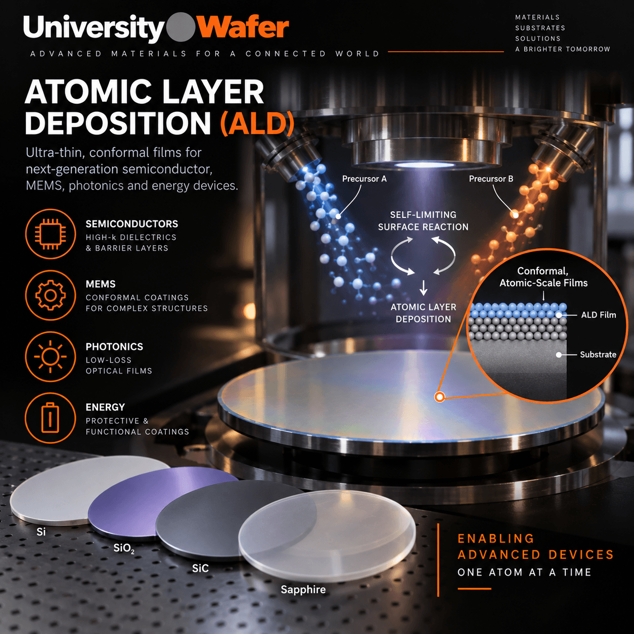
Unlike conventional deposition methods that continuously introduce reactive gases, ALD exposes the substrate to individual chemical precursors in a controlled sequence. Each precursor reacts with available surface sites through a self-limiting reaction, allowing researchers to build a thin film one cycle at a time.
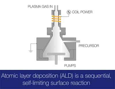 A typical ALD cycle consists of four main steps. First, the substrate is exposed to the initial precursor. The precursor molecules react with available chemical sites on the substrate surface. Once those sites are occupied, the reaction naturally stops.
An inert purge gas, such as nitrogen or argon, is then introduced to remove excess precursor molecules and reaction byproducts. A second precursor is introduced and reacts with the chemically modified surface. Another purge step removes the remaining gases before the cycle begins again.
Because each reaction is self-limiting, the amount of material deposited during every cycle is highly repeatable. The final film thickness can therefore be controlled by adjusting the total number of ALD cycles.
Basic Steps in an ALD Cycle
- First precursor exposure: The first precursor reacts with active sites on the substrate surface.
- First purge: An inert gas removes excess precursor molecules and gaseous reaction products.
- Second precursor exposure: The second reactant reacts with the surface created during the first exposure.
- Second purge: Excess reactants and byproducts are removed before the next cycle begins.
These steps are repeated until the desired film thickness is achieved. Depending on the material system and process conditions, each cycle may deposit a fraction of a nanometer of material.
Why Is ALD Used for Thin-Film Deposition?
Atomic layer deposition is particularly useful when a device requires an ultra-thin coating with excellent uniformity, controlled composition, and consistent coverage over complex surfaces. ALD films can coat flat wafers, trenches, pores, high-aspect-ratio structures, and three-dimensional device features.
Important advantages of the ALD process include:
- Precise film-thickness control at the nanometer scale
- Excellent conformality over complex three-dimensional structures
- Uniform coating across large substrate areas
- Repeatable and self-limiting surface reactions
- Low defect density when the process is properly optimized
- Compatibility with many metals, oxides, nitrides, and semiconductor materials
- Ability to deposit multilayers, nanolaminates, and compositionally controlled films
Common ALD materials include aluminum oxide, hafnium oxide, titanium oxide, zinc oxide, silicon oxide, silicon nitride, titanium nitride, and selected metallic films. The exact film chemistry depends on the precursors, reactants, substrate surface, temperature, and reactor design.
What Is Electrochemical Atomic Layer Deposition?
Electrochemical atomic layer deposition, sometimes called electrochemical ALD or EC-ALD, is a surface-limited electrochemical technique used to deposit extremely thin layers of material onto conductive substrates.
Unlike conventional vapor-phase ALD, electrochemical ALD generally takes place in a liquid electrolyte. The substrate acts as an electrode, and the deposition process is controlled through electrochemical potential, surface reactions, and sequential exposure to different chemical species.
EC-ALD can be used to investigate metals, compound semiconductors, multilayer structures, and nanostructured films. Potential research applications include:
- Infrared detectors
- Photovoltaic and solar-cell materials
- Thermoelectric devices
- Electrocatalysts
- Battery and energy-storage electrodes
- Metal and semiconductor superlattices
- Nanoscale electronic and optoelectronic devices
Electrochemical ALD should not be confused with standard thermal or plasma-enhanced ALD. Although both approaches rely on controlled, surface-limited reactions, they use different reaction environments and deposition mechanisms.
ALD Substrates and Surface Preparation
The substrate plays an important role in atomic layer deposition because ALD begins with chemical reactions at the substrate surface. Surface composition, cleanliness, roughness, native oxide, functional groups, and contamination can all affect nucleation and film growth.
Common substrates used for ALD research include:
- Silicon wafers
- Thermal oxide-coated silicon wafers
- Silicon-on-insulator wafers
- Sapphire substrates
- Silicon carbide wafers
- Gallium arsenide substrates
- Gallium nitride substrates
- Germanium wafers
- Glass and fused-silica substrates
- Metal-coated and patterned wafers
Prime-grade wafers may be preferred for advanced device fabrication, while test-grade, mechanical-grade, or reclaimed wafers can provide a cost-effective option for ALD process development, tool qualification, coating trials, and preliminary material characterization.
Atomic Layer Deposition vs. Chemical Vapor Deposition
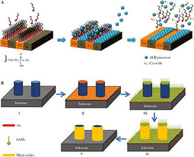 Atomic layer deposition and chemical vapor deposition (CVD) are both vapor-phase methods used to deposit thin films. However, they differ significantly in how the chemical precursors are introduced and how the film grows.
In ALD, the precursors are introduced separately and are divided by purge steps. Each precursor reacts with the surface through a self-limiting mechanism. This sequential process provides precise thickness control and excellent coating uniformity, even on complex three-dimensional structures.
In conventional CVD, multiple reactive gases are generally present in the deposition chamber at the same time. The gases react continuously at or near the heated substrate surface, allowing material to grow more rapidly.
Key Differences Between ALD and CVD
| Process Feature | Atomic Layer Deposition | Chemical Vapor Deposition |
|---|---|---|
| Precursor delivery | Precursors are introduced sequentially and separated by purge steps. | Reactive gases are generally introduced simultaneously or continuously. |
| Reaction mechanism | Surface-controlled and self-limiting. | Continuous chemical reaction at or near the substrate surface. |
| Thickness control | Controlled through the number of deposition cycles. | Controlled mainly through deposition time, temperature, pressure, and gas flow. |
| Deposition rate | Generally slower. | Generally faster. |
| Conformality | Excellent on high-aspect-ratio and three-dimensional structures. | Varies according to the process chemistry and reactor conditions. |
| Typical film thickness | Well suited for ultra-thin and nanoscale films. | Well suited for both thin and relatively thick films. |
| Material efficiency | Precise growth, although purge cycles can increase process time. | Higher throughput but may use more precursor material. |
| Common applications | High-k dielectrics, barrier films, advanced transistors, MEMS, batteries, and nanostructures. | Epitaxial layers, dielectric films, conductive coatings, solar cells, and semiconductor manufacturing. |
When Should Researchers Use ALD?
ALD is often selected when film thickness, conformality, interface quality, or nanoscale control is more important than deposition speed. It is especially valuable for coating narrow trenches, porous materials, nanowires, particles, and complex device structures that may be difficult to coat uniformly using conventional CVD or physical vapor deposition.
CVD may be more appropriate when a faster deposition rate, thicker film, or higher manufacturing throughput is required. The best method depends on the desired material, substrate, geometry, film thickness, process temperature, and final device application.
Applications of Atomic Layer Deposition
Atomic layer deposition is used across a wide range of scientific and industrial fields, including:
- High-k gate dielectrics for transistors
- Passivation and protective barrier coatings
- MEMS and microelectronic devices
- Solar cells and photovoltaic research
- Photodetectors and infrared sensors
- Battery electrodes and solid-state electrolytes
- Catalysts and electrocatalysts
- Optical coatings
- Quantum devices
- Three-dimensional semiconductor structures
- Nanowires, nanoparticles, and porous materials
Selecting the correct wafer material, diameter, surface finish, orientation, resistivity, oxide thickness, and grade can help researchers improve ALD nucleation, film uniformity, adhesion, and characterization results.
Related Pages
- Silicon Wafers – Prime, test, and mechanical-grade silicon substrates for ALD and semiconductor research.
- Thermal Oxide Silicon Wafers – Silicon substrates with high-quality SiO₂ layers for dielectric and ALD thin-film studies.
- TEOS Oxide Wafers – PECVD and TEOS oxide-coated wafers for dielectric deposition and semiconductor fabrication.
- Silicon Nitride Wafers – LPCVD and PECVD nitride-coated wafers used in MEMS, passivation, and ALD research.
- Silicon-on-Insulator (SOI) Wafers – High-performance substrates for MEMS, photonics, and advanced semiconductor devices.
- Silicon Epitaxial Wafers – Epitaxial silicon substrates for transistor, sensor, and integrated circuit fabrication.
- Silicon Carbide (SiC) Wafers – Wide-bandgap substrates for power electronics and high-temperature devices.
- GaN on Sapphire Wafers – Ideal substrates for LEDs, UV photodetectors, RF devices, and ALD thin-film research.
- Gallium Arsenide (GaAs) Wafers – Compound semiconductor substrates for high-speed electronics and optoelectronics.
- Sapphire Wafers – High-purity Al₂O₃ substrates widely used for ALD, epitaxy, optics, and semiconductor applications.
- Research Substrates – Browse semiconductor substrates for thin-film deposition, nanotechnology, and materials science.
- Photodetector Substrates – Materials for infrared, UV, and visible photodetector development using ALD coatings.