Benefits of Spin-on-Glass (SOG) Coatings
Spin-on-glass coatings can provide a practical route to dielectric insulation and wafer surface planarization. The liquid coating can flow into shallow surface features before curing, making SOG useful for selected semiconductor processing applications. Film quality and thickness depend on the SOG formulation, spin speed, substrate topography, and bake or cure schedule.
A researcher requested the following quote:
"I'm looking for a spin-on glass (SOG) material that can be spin- coated with a micrometer thickness of (2~5 microns). Can I get this thickness using your product by a single spin-coating or multiple spin-coatings? Is your SOG's refractive index closed to fused silica (quartz) or HSQ?"
Compared to gas diffusion doping, Spin-on doping uniformity is better. The variance across a wafer is between 0.5% and 1% and variance from wafer to wafer ranges between 1% - 2%.
Reference #265115 for specs and pricing. Buy as few as one wafer online and start researching today!
Get Your Quote FAST! Buy Online and Start Researching Today!
Spin-On-Glass Materials and Processing
Typical SOG processing involves dispensing a liquid precursor, spin coating it across the substrate, and performing controlled baking or curing. For projects requiring a silica-like coating, compare SOG with silicon dioxide (SiO2) and fused silica substrates. These are related materials, but their deposition methods and film properties are not interchangeable.
In addition, there are still many applications of spin-on glass technology, and these applications are gaining the various benefits discussed here. Spin on glass can satisfy new applications and their needs and can form compounds that differ in their chemical composition and properties. The substituents have a high binding energy to silica and dissolve when the spun glass layer is exposed to high temperatures during curing. [Sources: 3, 5]
In addition, the inventive TEOG - TEOS Spin - on glass has an additional advantage: there is no stress - altered flexibility of the glass based on spin. Through experiments, we have found that if processed correctly, the spinning glass described here can overcome the disadvantages mentioned above. In our work, a treated dielectric based on diluted deionized water as a viable solution for producing a powerful, cost-effective, and environmentally friendly spin on glasses.
What Is Spin-on-Glass (SOG)?
Spin-on-glass refers to coating materials that form a glass-like film after spin coating and thermal treatment. In microelectronics, these films may be used for gap filling, interlayer dielectric layers, and wafer planarization. For a comparison with vapor-deposited films, see chemical vapor deposition (CVD) and thermal silicon oxide.
Video Explaining Spin-on-Glass.
The planarized spin - on glass (SOG) - forms next to the first silicon oxide layer. The high selectivity of etching is crucial to remove the previous etching step and protect the metal from etching. In our work, the suction is applied to a glass layer and the CVD (silicon oxide barrier layer) is slowly etched. At the same time, the "etch recirculation" is carried out using reactive ion etching (RIE) under conditions that etch the SOG at the same speed as the glass layers, but at a much slower rate. [Sources: 1, 4, 8]
Another problem that makes etching - reprocessing - on glass layers more difficult is that the thick spinning film also detaches from the substrate during subsequent processing. Here the spin on glasses can become very thin and is a big step, which is connected with the use of stacked capacitors. Even in the case of a thin layer of etched spun glass, the exposed edges can lead to interlevel shorting and other reliability problems. Another problem that annoys the etch-back process is regions where a significant step is embedded in the underlying substrate, such as on the surface of the glass layer. [Sources: 1, 3]
Spin on glass can become quite thin when using the spin-coater process, especially with thin glass layers. [Sources: 1]
The spin - on glass composition in this invention is stable, even if it is increased to a temperature of more than 1,000 degrees Celsius. The reaction, which lasts two hours or more at ambient temperature, will effectively influence the composition of the glasses. Spin of glass occurs in alloys that are known to be resistant to the effects of high temperatures, such as high pressure, high heat and high humidity. At minus degrees there is no significant effect on the properties of the alloy or on its magnetism, which seems to be practically unused in daily life. [Sources: 2, 3, 7]
The present invention concerns a coating solution using a semiconductor product commonly referred to as spin - on glass composition. This is a liquid silicon mixture that can be applied to the surface of semiconductors on a wafer and then spun to create the coating layer on the top. In this technique, the spin on the glass composition fills the recessed areas of the wafer resulting from various insulating and conductive regions. For example, a spin of glass materials can be either a siloxane - a base material marketed under the trade name accuglass by Allied Signal Corp. - or a glass - a material such as glass. [Sources: 1, 3]
Although the spin on glass as a liquid precursor has a levelling effect, the thickness fluctuates greatly due to the underlying substrate. [Sources: 1, 3]
Spin-on Silicon-Based Dielectric Films
Silicon-based dielectric layers are important in semiconductor isolation and multilayer device processing. Compare SOG coating behavior with silicon nitride films and TEOS-derived silicon oxide when planning the required electrical and processing properties.
One disadvantage of spin on the glass composition is that it cannot control the plasma etching rate or the produced layer, as it is sensitive to the O 2 concentration. This minimises the micro-loading that would otherwise lead to non-flat surfaces that would be created by micro-loading. Although gasification can be eliminated by removing the metal, a number of other problems associated with etching on the back may occur, some of which are normally carried out with a plasma etching device, such as lack of selectivity. [Sources: 1, 3]
Sources:
[0]: https://shibaura.pure.elsevier.com/en/publications/spin-on-glass-film-treatment-technology-using-a-fluoroalkoxysilan
[1]: https://www.google.fr/patents/US5461010
[3]: https://patents.google.com/patent/US5152834A/en
[4]: https://www.freepatentsonline.com/5747381.html
[5]: http://www.google.com/patents/US5910680
[6]: http://www.scielo.org.mx/scielo.php?script=sci_arttext&pid=S0035-001X2016000300282
[8]: https://www.google.com.na/patents/US5631197
[9]: https://www.science.gov/topicpages/s/spin-on+glass+sog.html
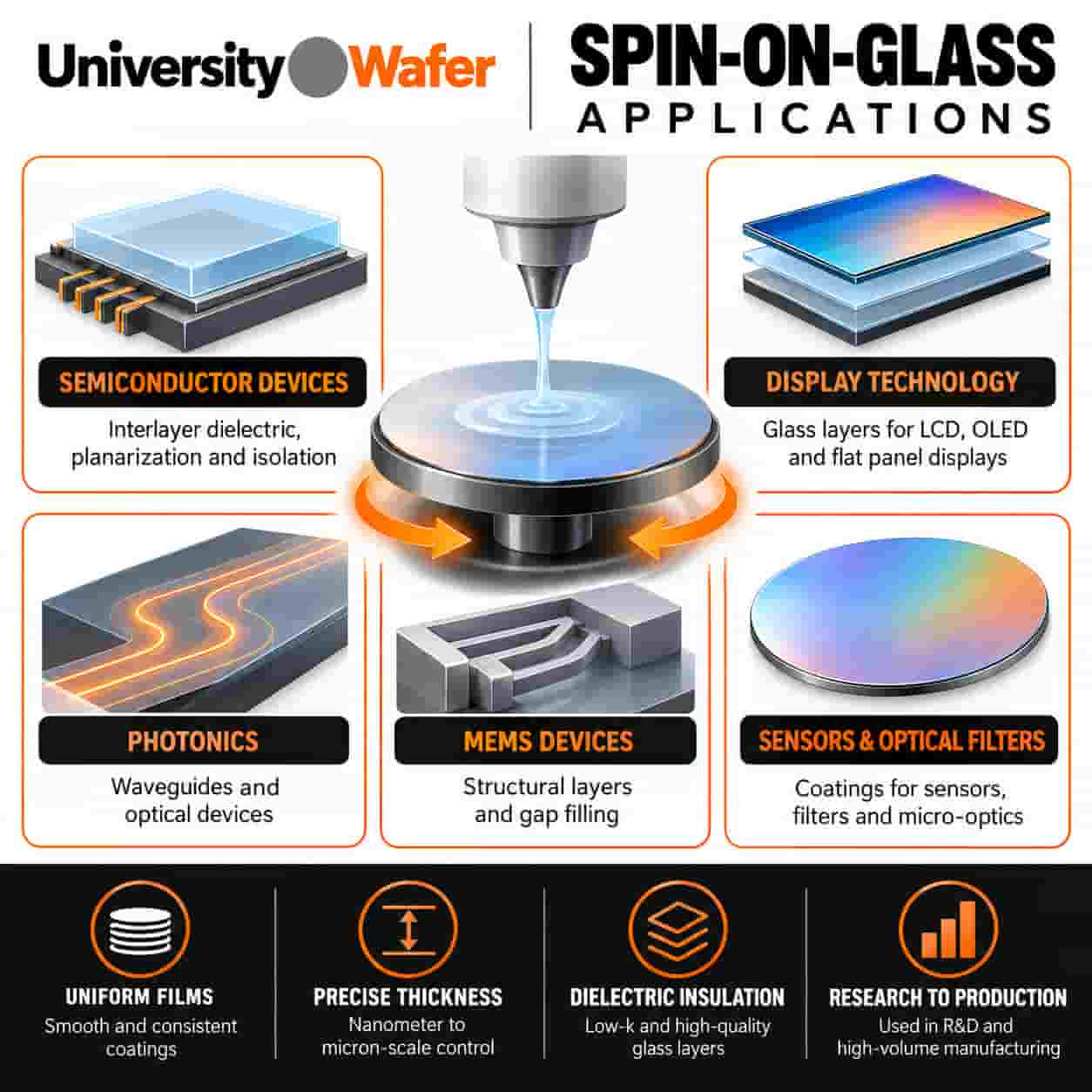
Spin-on-Glass Applications in Semiconductor Fabrication
Spin-on-glass (SOG) is used in semiconductor and microfabrication processes
where a smooth, uniform dielectric coating is needed. Common applications include
planarization, gap filling, photonics, MEMS, display technology, sensors, and optical devices.
SOG materials can help create thin insulating layers with controlled thickness while
supporting both research-scale processing and semiconductor manufacturing.
- Heavy Aluminium doped spin-on glass silica
- Medium Arsenic doped spin-on glass silica
- 300 Non-doped spin-on glass silica
- Medium Boron doped spin-on glass silica
- Heavy Boron doped spin-on glass silica
- Heaviest Boron doped spin-on glass silica
- Lightly Boron doped spin-on glass silica *available in ultrahigh purity only
- Heavy Barium doped spin-on glass silica
- Heavy Gallium doped spin-on glass silica
- Heavy Gallium Aluminium doped compound spin-on glass silica
- Heavy Indium doped spin-on glass silica
- Heavy Lithium doped spin-on glass silica
- Heavy lithium phosphorous doped compound spin-on glass.
- Magnesium doped spin-on glass silica
- 2000A Non-doped spin-on glass silica
- 3000 Non-doped spin-on glass silica
- 5000A Non-doped spin-on glass silica
- 7000A Non-doped spin-on glass silica
- Lightly Phosphorous doped spin-on glass silica
- Medium Phosphorous doped spin-on glass silica
- Heavy Phosphorous doped spin-on glass silica
- Heaviest Phosphorous doped spin-on glass silica
- Heavy Antimony doped spin-on glass silica
- Heavy Tin doped spin-on glass silica
- Lightly Silica-doped spin-on glass titanate
- Compound Spin-on glass titanate/silica
- 1000A Non-doped spin-on glass titanate
- Medium Zinc doped spin-on glass silica
- Heavy Zinc doped spin-on glass silica
- Heavy Zinc doped spin-on glass silica *ultrahigh purity
- Heavier Zinc doped spin-on glass silica
- Heavy Zinc Arsenic doped spin-on glass silica
- Heavy Zinc Phosphorous doped spin-on glass silica
Spin-on-Glass Planarization, Trench Filling and Masking
For patterned silicon wafers, SOG can help smooth topography and fill certain narrow features before subsequent processing. Coating uniformity, cracking, shrinkage, and thermal compatibility should be evaluated for the intended process.
- 300 Non-doped spin-on glass silica
- Heavy Boron doped spin-on glass silica
- Heavy Boron doped spin-on glass silica
- Heaviest Boron doped spin-on glass silica
- Heaviest Boron doped spin-on glass silica
- Light doped, compound SOG
- Heavy doped, compound SOG
- 500A Non-doped spin-on glass silica
- 800A Non-doped spin-on glass silica
- 1000A Non-doped spin-on glass silica
- 2000A Non-doped spin-on glass silica
- 3000 Non-doped spin-on glass silica
- 5000A Non-doped spin-on glass silica
- 7000A Non-doped spin-on glass silica
- Heavy Phosphorous doped spin-on glass silica
- Heaviest Phosphorous doped spin-on glass silica
- Heaviest Phosphorous doped spin-on glass silica
- Lightly Silica-doped spin-on glass titanate
- Compound Spin-on glass titanate/silica
- 1000A Non-doped spin-on glass titanate
- 1100A Non-doped spin-on glass titanate
- 300 Non-doped spin-on glass silica
- Heavy Neodymium doped high RI spin-on glass silica
- 500A Non-doped spin-on glass silica
- 800A Non-doped spin-on glass silica
- 1000A Non-doped spin-on glass silica
- 2000A Non-doped spin-on glass silica
- 3000 Non-doped spin-on glass silica
- 5000A Non-doped spin-on glass silica
- 7000A Non-doped spin-on glass silica
- 300 Non-doped spin-on glass silica
- 500A Non-doped spin-on glass silica
- 800A Non-doped spin-on glass silica
- 1000A Non-doped spin-on glass silica
- 2000A Non-doped spin-on glass silica
- 3000 Non-doped spin-on glass silica
- 5000A Non-doped spin-on glass silica
- 7000A Non-doped spin-on glass silica
Wafer Bonding
In research workflows, selected glass-like coatings may be evaluated as intermediate layers for silicon-on-insulator (SOI) and other wafer integration approaches. Bonding performance depends on material selection and process conditions.
- 300 Non-doped spin-on glass silica
- 500A Non-doped spin-on glass silica
- 800A Non-doped spin-on glass silica
- 1000A Non-doped spin-on glass silica
- 2000A Non-doped spin-on glass silica
- 3000 Non-doped spin-on glass silica
- 5000A Non-doped spin-on glass silica
- 7000A Non-doped spin-on glass silica
- Heavy Aluminium doped spin-on glass silica
- Medium Arsenic doped spin-on glass silica
- 300 Non-doped spin-on glass silica
- Medium Boron doped spin-on glass silica
- Heavy Boron doped spin-on glass silica
- Heaviest Boron doped spin-on glass silica
- Lightly Boron doped spin-on glass silica *available in ultrahigh purity only
- Heavy Barium doped spin-on glass silica
- Heavy Gallium doped spin-on glass silica
- Heavy Gallium Aluminium doped compound spin-on glass silica
- Heavy Indium doped spin-on glass silica
- Heavy Lithium doped spin-on glass silica
- Heavy lithium phosphorous doped compound spin-on glass
- Magnesium doped spin-on glass silica
- 2000A Non-doped spin-on glass silica
- 3000 Non-doped spin-on glass silica
- 5000A Non-doped spin-on glass silica
- 7000A Non-doped spin-on glass silica
- Lightly Phosphorous doped spin-on glass silica
- Lightly Phosphorous doped spin-on glass silica
- Medium Phosphorous doped spin-on glass silica
- Medium Phosphorous doped spin-on glass silica
- Heavy Phosphorous doped spin-on glass silica
- Heavy Phosphorous doped spin-on glass silica
- Heavy Phosphorous doped spin-on glass silica
- Heaviest Phosphorous doped spin-on glass silica
- Heaviest Phosphorous doped spin-on glass silica
- Heavy Antimony doped spin-on glass silica
- Heavy Tin doped spin-on glass silica
- Lightly Silica-doped spin-on glass titanate
- Compound Spin-on glass titanate/silica
- 1000A Non-doped spin-on glass titanate
- 1100A Non-doped spin-on glass titanate
LED and Infrared (IR) Detector Applications
Research into optical and electronic devices may use insulating or functional spin-on films in conjunction with photonic devices and gallium arsenide substrates. Suitability must be verified for the device stack and thermal budget.
- Heavy Aluminium doped spin-on glass silica
- Medium Arsenic doped spin-on glass silica
- Medium Boron doped spin-on glass silica
- Medium Boron doped spin-on glass silica
- Heavy Boron doped spin-on glass silica
- Heavy Boron doped spin-on glass silica
- Heaviest Boron doped spin-on glass silica
- Heaviest Boron doped spin-on glass silica
- Lightly Boron doped spin-on glass silica *available in ultrahigh purity only
- Heavy Barium doped spin-on glass silica
- Heavy Gallium doped spin-on glass silica
- Heavy Gallium Aluminium doped compound spin-on glass silica
- Silicate gallium and boron doped glass
- Heavy Indium doped spin-on glass silica
- Heavy Lithium doped spin-on glass silica
- Heavy lithium phosphorous doped compound spin-on glass.
- Magnesium doped spin-on glass silica
- Lightly Phosphorous doped spin-on glass silica
- Lightly Phosphorous doped spin-on glass silica
- Medium Phosphorous doped spin-on glass silica
- Medium Phosphorous doped spin-on glass silica
- Heavy Phosphorous doped spin-on glass silica
- Heavy Phosphorous doped spin-on glass silica
- Heavy Phosphorous doped spin-on glass silica
- Heaviest Phosphorous doped spin-on glass silica
- Heavy Antimony doped spin-on glass silica
- Heavy Tin doped spin-on glass silica
- Medium Zinc doped spin-on glass silica
- Heavy Zinc doped spin-on glass silica
- Heavy Zinc doped spin-on glass silica *ultrahigh purity
- Heavier Zinc doped spin-on glass silica
- Heavy Aluminium doped spin-on glass silica
- Medium Arsenic doped spin-on glass silica
- 300 Non-doped spin-on glass silica
- Medium Boron doped spin-on glass silica
- Heavy Boron doped spin-on glass silica
- Heavy Boron doped spin-on glass silica
- Heaviest Boron doped spin-on glass silica
- Heaviest Boron doped spin-on glass silica
- Lightly Boron doped spin-on glass silica *available in ultrahigh purity only
- Heavy Barium doped spin-on glass silica
- Heavy Gallium doped spin-on glass silica
- Heavy Gallium Aluminium doped compound spin-on glass silica
- Heavy Indium doped spin-on glass silica
- Heavy Lithium doped spin-on glass silica
- Heavy lithium phosphorous doped compound spin-on glass.
- Magnesium doped spin-on glass silica
- 2000A Non-doped spin-on glass silica
- 3000 Non-doped spin-on glass silica
- 5000A Non-doped spin-on glass silica
- 7000A Non-doped spin-on glass silica
- Lightly Phosphorous doped spin-on glass silica
- Lightly Phosphorous doped spin-on glass silica
- Medium Phosphorous doped spin-on glass silica
- Medium Phosphorous doped spin-on glass silica
- Heavy Phosphorous doped spin-on glass silica
- Heavy Phosphorous doped spin-on glass silica
- Heavy Phosphorous doped spin-on glass silica
- Heaviest Phosphorous doped spin-on glass silica
- Heaviest Phosphorous doped spin-on glass silica
- Heavy Antimony doped spin-on glass silica
- Heavy Tin doped spin-on glass silica
- Lightly Silica-doped spin-on glass titanate
- Compound Spin-on glass titanate/silica
- 1000A Non-doped spin-on glass titanate
Superconductor Precursor Research
- Heavy Barium doped spin-on glass silica
- Heavy Copper doped spin-on glass silica
- Heavy Yttrium doped spin-on glass silica
- Heavy Yittrium Barium Copper doped compound spin-on glass silica superconductor precursor
Related Spin-on-Glass & Semiconductor Resources
