Porous Silicon Wafers for Research & Production
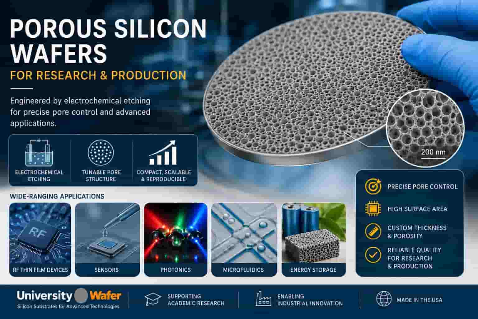
Porous silicon is a silicon wafer surface engineered with nanoscale or microscale pores, typically formed through electrochemical etching (anodization). Because pore size, porosity, and thickness can be tuned, porous silicon wafers are widely used in research for RF thin film devices, optical and biosensing platforms, photonics, microfluidics, and energy storage. This page summarizes porous silicon fabrication methods, common wafer specifications, and real-world applications to help researchers select the right porous silicon substrate for their experiments.
Porous Silicon for RF Thin Film Devices
A PhD student need a quote for the following:
I a PhD student working on the development of RF thin film devices. I am currently exploring using porous silicon in my research and came across your company’s products. I am interested in learning more about your porous silicon wafer offerings, specifically regarding:
- Available specifications of the Porous diameter
- Distance between them
- Thickness Customization option
If any Pricing details for research quantities Lead time for delivery Your assistance in providing this information would be greatly appreciated, as it will help me determine the suitability of your products for my project. Thank you for your time and support. I look forward to your response.
Reference #320311 for specs and pricing.
Porous Silicon Wafer
The following wafer spec has been used in experiments. 100mm silicon wafer N/Ph (100) 150µm 1–2 Ω cm SSP.
 The novel uses of porous silicon include powering sattelites and perhaps even space ships!
In the early 2000s scientists discoverd that hydrogenated porous silicon reacts explosively with oxygen at very low (cryogenic) temperatures. A porous silicon wafer in say outer space would release several times as much energy as an equivalent amount of dynamite, and at a much greater speed. The properties of the porous silicon and how it handles oxygen very well. This allows for a fats and even detonation.
Currently porous silicon is being researched as a potential thrusting mechanism for satellites.
Get Your Quote FAST! Or, Buy Online and Start Researching Today!
Porous Silicon Discovery
In 1956 porous silicon was first discovered. The material gained importance in the 1990s when two optical properties were discovered. In the study of transmembrane proteins, a porous silicon membrane of 3 micrometers diameter was produced, which produced a high-resolution image of the surface of a single protein.
Electrochemical Impedance Spectroscopy (EIS) investigated the protein and the experiment was published in the Journal of The American Chemical Society (ACS) journal ACS Nano in June 2014.
The experimental process required the development of a porous silicon membrane, followed by the synthesis of an epithelial sodium channel protein (ENaC) in Langmuir - Blodgett - Lang Muir and Schafer technique. Finally, the epithelium - sodium - channel - protein EN aC was fused to form a lipid two-layer membrane.
The functioning of the device was investigated by means of electrochemical impedance spectroscopy (EIS) and magnetic resonance imaging (MRA).
Wafers Used for Electrochemical Etching to Obtain Porous Silicon Particles
A scientist asked us which silicon wafer spec is used to obtain porous silicon particles.
We quoted the following:
Si Item #1116
100mm P/B (100) 10-20 ohm-cm SSP Prime Grade and we deposited an Al Layer on Backside in order to have an ohmic contact
Please contact us for a quote.
How to Make Rugate Optical Filters Using Porous Silicon
Etching Silicon Wafers to make colorful Rugate Optical Filters
Important Porous Silicon Terms
The following are some porous silicon keywords.
- porous silicon
- metallic nanostructures
- electrochemical etching
- anodic silicon
- silicon wafers
- silicon layers
- silicon nanocrystallites
- silicon surfaces
- silicon structures
- silicon substrate
- silicon fabrication
- silicon atoms
- electrochemical anodization
- crystalline silicon
- silicon formation
- optical biosensor
How to Fabricate Porous Silicon
Fabrication method
The fabrication method of porous silicon focuses on the layering of p-Si or AgNPs. Using a vacuum holding and pulling technique, large silicon wafers are etched in an electrochemical cell. A porous silicon layer is then ''deposited'' on the as-prepared solar cell, which improves the efficiency of the cell. The process has the potential to be used in energy storage and photovoltaic devices.
The fabrication method of porous Si is relatively simple. Electrochemical etching of porous silicon produces porous silicon with a varying pore size. Pore size can be controlled by changing the current density. Larger pore sizes are preferable for large molecules or drugs. The larger the pore size, the faster the host matrix degrades. The fabrication protocol of porous silicon is detailed in the publications.
A second porous silicon fabrication method involves a layer transfer technique. This method requires the use of anodizing a silicon substrate in order to enable the formation of thick silicon layers. The first porous layer is fabricated with a low porosity, and the second layer is formed with a high-porosity layer. The device layer is then fused to the handle substrate using high-temperature argon annealing.
During the formation of porous silicon, hydrogen will be evolved. The introduction of absolute ethanol to the solution will eliminate hydrogen. The introduction of ethanol will improve the infiltration of HF solution into pores and will result in a more uniform distribution of thickness and porosity. Lastly, alcohol adsorption enhances the diffusion process and enables the formation of the porous silicon layer. So, if you are looking for a porous silicon fabrication method, read on!
The pore geometry depends on the crystalline orientation. For instance, a hundred-cut Si crystal has perpendicular pores. On the other hand, Si (001) has perpendicular pores. Therefore, the pore geometry of 100-cut silicon depends on its orientation. The pore geometry and architecture of a porous layer are crucial for the pore formation. The fabrication method for porous silicon is still a relatively young process but it is one that is gaining a lot of attention in the last decade.
Porous Silicon for ZnO Thin Film Research
Porous silicon (PS) has become one of the most widely studied semiconductor substrates for depositing
ZnO (zinc oxide) thin films. The combination of a high surface area, tunable
porosity, and excellent optical properties makes porous silicon an attractive material for
research involving optoelectronics, photodetectors, gas sensors, biosensors, solar cells, and advanced semiconductor devices.
Researchers frequently deposit ZnO thin films onto porous silicon using techniques such as
sol-gel processing, dip coating, sputtering, atomic layer deposition (ALD), and chemical vapor deposition (CVD).
After deposition, the films are characterized to determine how the porous surface influences their structural,
electrical, and optical performance.
Important Optical Properties Measured
Scientific studies commonly evaluate porous silicon and ZnO-coated porous silicon using the following optical
and electrical parameters:
| Property |
Research Importance |
| Refractive Index |
Determines how light propagates through porous silicon and ZnO films. |
| Absorption Coefficient |
Measures how efficiently the material absorbs ultraviolet and visible light. |
| Energy Gap (Band Gap) |
Used to evaluate electronic and optoelectronic performance. |
| Optical Conductivity |
Provides insight into photon interaction and carrier generation. |
| Electrical Conductivity |
Determines charge transport characteristics for electronic devices. |
| Surface Roughness |
Influences thin-film adhesion, crystal growth, and optical scattering. |
AFM Surface Characterization
One of the most common techniques used to characterize porous silicon is
Atomic Force Microscopy (AFM).
AFM provides high-resolution images of the porous surface and measures
surface roughness, pore diameter, pore distribution, and film uniformity before and after ZnO deposition.
These measurements help researchers optimize film growth and improve device performance.
Why Porosity Matters
The porosity of a porous silicon wafer directly affects its
refractive index, optical reflectance,
light absorption, and electrical behavior.
By controlling pore size and pore density during electrochemical etching,
researchers can engineer porous silicon substrates for specific photonic,
MEMS, sensing, and semiconductor applications.
Applications of ZnO on Porous Silicon
- Optical sensors
- Gas sensors
- UV photodetectors
- Solar cells
- Photonic devices
- MEMS and NEMS research
- Biomedical sensors
- Thin-film semiconductor devices
Related UniversityWafer Resources
