
Buy 200mm (8-Inch) Silicon Wafers Online
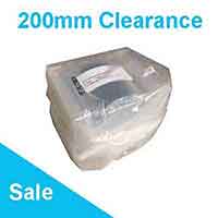 UniversityWafer supplies a broad selection of
silicon wafers
in the 200mm, or 8-inch, diameter format. Available options may include
prime-grade, test-grade, mechanical-grade, Czochralski-grown, and Float Zone silicon wafers
for semiconductor fabrication, equipment testing, thin-film deposition, MEMS, lithography,
spin coating, and materials research.
UniversityWafer supplies a broad selection of
silicon wafers
in the 200mm, or 8-inch, diameter format. Available options may include
prime-grade, test-grade, mechanical-grade, Czochralski-grown, and Float Zone silicon wafers
for semiconductor fabrication, equipment testing, thin-film deposition, MEMS, lithography,
spin coating, and materials research.
In-stock wafers can often ship quickly in research and production quantities. For custom specifications, provide the required grade, orientation, dopant, resistivity, thickness, polish, quantity, and application in the quote form below.
Example 200mm Silicon Wafer Specifications
- Diameter: 200 ± 0.5mm
- Conductivity: P-type silicon
- Crystal orientation: <100>
- Resistivity: 1,000–3,000Ω·cm
- Thickness: 705–745µm
- Edge identification: V-notch
- Surface: Polished/etched
- Packaging: 25 wafers per cassette in a sealed foil bag
Specifications and availability change frequently. Contact us for current inventory, small-quantity availability, custom processing, or volume pricing.
Get Your 200mm Silicon Wafer Quote FAST! Or, Buy Online and start researching today!
200mm Silicon Wafers for Magnetic-Field Research
Silicon substrates may be used in experiments involving strong or pulsed magnetic fields, including Hall-effect measurements, magnetotransport studies, quantum-device research, thin-film characterization, and sensor fabrication. The magnetic field does not produce the wafer or perform the sputtering process; instead, researchers expose a fabricated semiconductor sample to the field and measure changes in its electrical behavior.
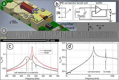
Important wafer properties for magnetic-field experiments may include conductivity type, carrier concentration, mobility, resistivity, crystal orientation, wafer thickness, surface finish, and dopant uniformity. High-resistivity or Float Zone silicon may be preferred when low impurity levels, low parasitic conduction, or long carrier lifetime are important.
Thin films such as metals, dielectrics, magnetic materials, graphene, or other semiconductor layers may be deposited on the silicon before the sample is patterned and tested. Suitable deposition methods include sputtering, evaporation, chemical vapor deposition, and atomic layer deposition.
200mm Silicon Wafers for Polymer Spin Coating
The flat, circular surface of an 8-inch silicon wafer makes it a useful substrate for spin coating photoresists, polyimides, SU-8, polymers, sol-gel materials, and other liquid films. Spin coating distributes a liquid across the wafer using centrifugal force to create a thin and relatively uniform coating.
The most appropriate wafer grade depends on the purpose of the experiment. Test-grade silicon wafers and mechanical-grade wafers may be economical choices for coating trials, equipment setup, process training, and non-device tests. Prime-grade wafers are generally preferred for photolithography, fine patterning, and experiments where surface defects or particles could affect the results.
Important Specifications for Spin Coating
- Surface finish: SSP or DSP
- Surface condition: Clean, polished, and low in particles
- Flatness: Suitable bow, warp, and total thickness variation
- Thickness: Compatible with the chuck and handling system
- Edge profile: Appropriate for secure vacuum-chuck contact
- Wafer grade: Prime, test, reclaim, or mechanical
- Surface film: Bare silicon, thermal oxide, nitride, or another coating
Coating uniformity can be influenced by spin speed, acceleration, solution viscosity, dispense volume, solvent evaporation, wafer temperature, surface energy, and wafer topography. Features such as trenches, steps, or patterned structures may cause material to accumulate in recessed areas or become thinner near raised edges.
Recommended Wafer Options
Researchers commonly select the following 200mm substrates for coating experiments:
- Mechanical-grade 200mm silicon, approximately 750µm thick, SSP
- Test-grade 200mm silicon for photoresist and polymer process development
- Prime-grade 200mm silicon for lithography and device fabrication
- Thermal oxide silicon wafers for dielectric or surface-chemistry studies
- Thin silicon wafers for flexible-device, backside-processing, or packaging research
For repeatable coating results, use wafers with consistent thickness, polish, surface preparation, and dimensional tolerances across each experimental batch.
Choosing CZ or Float Zone 200mm Silicon
Most standard 200mm wafers are produced using the Czochralski growth method. CZ silicon is widely available in many dopant, resistivity, orientation, and polish options, making it suitable for integrated circuits, MEMS, thin-film deposition, oxidation, lithography, and general semiconductor research.
Float Zone silicon generally contains less oxygen and carbon and is available in high-resistivity specifications. It may be selected for radiation detectors, RF devices, power electronics, high-field experiments, and other applications requiring high-purity silicon.
Related Wafer Sizes and Materials
Researchers evaluating 200mm silicon substrates may also compare:
- 100mm silicon wafers for early-stage research and smaller fabrication tools.
- 150mm silicon wafers for legacy tools, university cleanrooms, and pilot-line processing.
- 300mm silicon wafers for advanced semiconductor process development and high-volume manufacturing.
- Silicon-on-insulator wafers for MEMS, RF, photonics, power electronics, and advanced CMOS devices.
- High-resistivity silicon wafers for RF, detector, and low-loss research.
- Silicon carbide wafers for high-power, high-temperature, and wide-bandgap semiconductor devices.
- Sapphire wafers for optical, RF, GaN epitaxy, and high-temperature applications.
What Are 200mm Silicon Wafers Used For?
200mm silicon wafers, also called 8-inch silicon wafers, are widely used for semiconductor research, pilot production, equipment qualification, process development, and commercial device fabrication. Their large usable surface area allows many dies, sensors, or test structures to be fabricated on a single wafer while remaining compatible with established 200mm semiconductor equipment.
UniversityWafer supplies silicon wafers in prime, test, reclaim, and mechanical grades with a variety of dopants, resistivities, crystal orientations, thicknesses, and surface finishes.
Common applications for 200mm wafers include:
- Integrated circuits and CMOS devices — microcontrollers, analog circuits, power-management devices, memory components, and mature-node semiconductor products.
- MEMS fabrication — accelerometers, pressure sensors, microphones, actuators, resonators, and microfluidic devices.
- Power electronics — MOSFETs, diodes, insulated-gate devices, and high-voltage semiconductor structures.
- Optoelectronics — image sensors, photodetectors, optical test structures, and silicon photonic devices.
- Thin-film research — sputtering, evaporation, chemical vapor deposition, atomic layer deposition, and polymer spin coating.
- Equipment testing — process-tool calibration, wafer handling, chuck testing, deposition uniformity studies, and automated inspection.
Why Choose 200mm Wafers?
A 200mm wafer provides substantially more usable surface area than a 150mm silicon wafer, while generally requiring less expensive tooling and infrastructure than a 300mm silicon wafer. This makes the 8-inch format especially useful for mature semiconductor processes, university cleanrooms, pilot lines, MEMS foundries, and specialty-device manufacturers.
The 200mm format is also supported by a large installed base of lithography, oxidation, diffusion, deposition, etching, metrology, and wafer-handling equipment.
200mm Silicon Wafer Grades
The appropriate wafer grade depends on the device, process step, and required surface quality. UniversityWafer can help researchers select among the following common options:
Prime-Grade 200mm Silicon Wafers
Prime-grade wafers are used for demanding semiconductor fabrication where low particle levels, tight dimensional tolerances, excellent flatness, and a high-quality polished surface are required. They are commonly selected for photolithography, device fabrication, epitaxy, oxidation, thin-film deposition, and advanced research.
Test-Grade 200mm Silicon Wafers
Test-grade silicon wafers provide a cost-effective substrate for process development, equipment calibration, deposition trials, wafer handling, spin coating, and non-device experiments.
Mechanical-Grade and Reclaim Wafers
Mechanical-grade and reclaim wafers are frequently used for tool setup, robotic handling tests, chamber seasoning, thermal-process trials, sputtering, training, and applications where electronic-grade surface quality is not required.
Common 200mm Silicon Wafer Specifications
Standard and custom 8-inch silicon wafer specifications may include:
- Diameter: 200mm, commonly specified with a tight diameter tolerance
- Thickness: approximately 650–750µm for standard wafers
- Crystal orientation: <100> or <111>
- Conductivity type: p-type, n-type, or undoped
- Dopants: boron, phosphorus, arsenic, or antimony
- Resistivity: heavily doped through high-resistivity ranges
- Surface finish: single-side polished (SSP) or double-side polished (DSP)
- Edge identification: notch, typically a V-notch for 200mm wafers
- Growth method: Czochralski (CZ), magnetic Czochralski, or Float Zone (FZ)
- Optional films: thermal oxide, silicon nitride, metals, or deposited dielectric layers
Thin 200mm Silicon Wafers
Thin 200mm silicon wafers are available for research involving flexible electronics, power devices, MEMS, backside processing, wafer bonding, packaging, thermal management, and weight-sensitive systems.
Common custom thickness requests include:
- 75µm
- 100µm
- 125µm
- 150µm
- Other custom thicknesses upon request
Thin wafers require careful handling because reduced thickness increases the risk of bow, breakage, edge damage, and handling-tool incompatibility. Temporary bonding, specialty carriers, or protective packaging may be recommended for some processes.
200mm Silicon Wafers for Polymer Spin Coating
200mm silicon wafers are commonly used as substrates for spin coating photoresists, polyimides, SU-8, polymers, sol-gel materials, and other liquid films. A flat, uniformly polished surface helps produce consistent film thickness across the wafer.
Mechanical-grade or test-grade wafers may be suitable for early coating trials, while prime-grade wafers are generally preferred when surface defects, particles, flatness, or coating uniformity can affect the final result.
Important spin-coating wafer specifications include:
- Wafer diameter and thickness
- Single-side or double-side polish
- Surface roughness
- Total thickness variation (TTV)
- Bow and warp
- Edge profile and notch position
- Surface cleanliness and particle count
- Compatibility with the spin-coater chuck
Researchers can buy 200mm silicon wafers online or request custom specifications for polymer and photoresist coating experiments.
Measuring Carrier Concentration and Mobility
Carrier concentration and carrier mobility are important electrical properties of doped silicon. They influence wafer resistivity, conductivity, device switching behavior, current flow, and overall semiconductor performance.
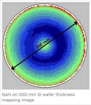
Common characterization methods include:
- Hall-effect measurement — determines carrier type, sheet carrier concentration, and mobility.
- Four-point probe measurement — measures sheet resistance without relying on contact resistance from a two-probe configuration.
- Spreading resistance profiling — evaluates resistivity or dopant concentration as a function of depth.
- Contactless resistivity mapping — measures wafer-level resistivity uniformity without fabricating permanent electrical contacts.
- Capacitance-voltage testing — evaluates semiconductor doping and dielectric-interface properties in fabricated test structures.
Measurements may be taken at the center and at multiple radial locations to evaluate wafer uniformity. The appropriate method depends on the resistivity range, sample geometry, wafer thickness, surface condition, and whether the wafer contains deposited films.
200mm Silicon Wafers for Hall-Effect Research
Hall-effect experiments require more than selecting a wafer by diameter alone. Researchers should specify the electrical and physical properties that influence carrier transport and measurement accuracy.
Important specifications may include:
- p-type or n-type conductivity
- Dopant species
- Target resistivity or carrier concentration
- Crystal orientation
- Wafer thickness
- Single-side or double-side polish
- Surface roughness and cleanliness
- Radial resistivity uniformity
- Required test-piece geometry
- Ohmic contact or metallization requirements
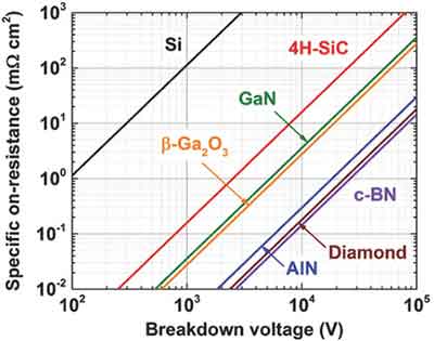
Full 200mm wafers may be used when wafer-scale mapping or compatibility with automated equipment is required. For conventional Hall measurements, however, the wafer is often diced into smaller square, rectangular, cross-shaped, or van der Pauw test samples before contacts are deposited.
UniversityWafer can provide full wafers or custom-diced silicon substrates for Hall-effect, conductivity, dopant, and semiconductor transport studies.
200mm Float Zone Silicon Wafers
Float Zone silicon wafers are manufactured using a localized molten zone that travels through a high-purity silicon rod. Because the process does not use a quartz crucible, FZ silicon generally contains less oxygen than conventional Czochralski-grown silicon.
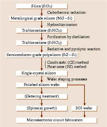
High-purity FZ silicon is frequently selected for high-resistivity substrates, power electronics, radiation detectors, RF devices, particle detectors, precision sensors, and scientific instrumentation.
Advantages of Float Zone silicon may include:
- Very low oxygen and carbon concentrations
- High bulk purity
- High-resistivity options
- Long minority-carrier lifetime
- Low defect and contamination levels
- Suitability for sensitive detector and power-device applications
Although smaller-diameter FZ wafers are more common, 200mm Float Zone silicon may be available in selected specifications. Diameter, resistivity, orientation, thickness, dopant, and quantity should be included when requesting a quote.
200mm Czochralski Silicon Wafers
Czochralski-grown silicon is the most widely available material for standard 200mm wafer production. During CZ growth, a seed crystal is withdrawn from molten silicon contained in a quartz crucible, producing a cylindrical single-crystal ingot.
CZ wafers are commonly used for integrated circuits, MEMS, sensors, power devices, thermal oxidation, thin-film deposition, lithography, and general semiconductor research. They are typically more readily available and economical than equivalent large-diameter Float Zone wafers.
200mm CZ vs. FZ Silicon
| Property | Czochralski Silicon | Float Zone Silicon |
|---|---|---|
| Availability | Widely available in 200mm | More limited at 200mm |
| Oxygen Content | Higher due to quartz crucible growth | Very low |
| Resistivity Range | Broad standard range | Excellent for high-resistivity material |
| Typical Applications | ICs, MEMS, sensors, general fabrication | Power devices, detectors, RF, scientific research |
| Relative Cost | Generally lower | Generally higher |
How to Select a 200mm Silicon Wafer
When requesting a quote, provide as many of the following specifications as possible:
- Quantity
- Prime, test, reclaim, or mechanical grade
- CZ or FZ growth method
- <100> or <111> orientation
- p-type, n-type, or undoped silicon
- Dopant species
- Target resistivity
- Wafer thickness
- SSP or DSP surface finish
- TTV, bow, warp, and flatness requirements
- Particle or surface-quality requirements
- Thermal oxide, nitride, metal, or other deposited films
- Full wafers or custom-diced pieces
Selecting the correct combination of grade, crystal orientation, resistivity, thickness, and surface finish helps ensure compatibility with your fabrication equipment and research process.
Related 200mm Silicon Wafer Resources
Explore related silicon wafer sizes, grades, growth methods, surface finishes, and specialty substrates for semiconductor fabrication and research.
- Silicon Wafers — Browse silicon substrates by diameter, orientation, dopant, resistivity, and surface finish.
- 100mm Silicon Wafers — A common format for university cleanrooms, MEMS research, and process development.
- 150mm Silicon Wafers — Suitable for legacy fabrication tools, pilot lines, and specialty semiconductor processes.
- 300mm Silicon Wafers — Large-diameter substrates for advanced process development and high-volume manufacturing.
- Test-Grade Silicon Wafers — Cost-effective wafers for equipment calibration, deposition trials, spin coating, and training.
- Thin Silicon Wafers — Custom-thickness substrates for MEMS, flexible electronics, packaging, and backside processing.
- Float Zone Silicon Wafers — High-purity, low-oxygen silicon for detectors, RF devices, and power electronics.
- Czochralski Silicon Wafers — Widely available CZ-grown silicon for ICs, MEMS, lithography, oxidation, and general research.
- P-Type Silicon Wafers — Boron-doped silicon substrates available in multiple resistivity and orientation ranges.
- N-Type Silicon Wafers — Phosphorus-, arsenic-, or antimony-doped wafers for electronic and sensor applications.
- High-Resistivity Silicon Wafers — Low-loss substrates for RF, microwave, detector, and high-field research.
- Thermal Oxide Silicon Wafers — Silicon substrates with wet or dry thermal SiO₂ for dielectric and device fabrication.
- Silicon-on-Insulator Wafers — SOI substrates for MEMS, RF, silicon photonics, power devices, and advanced CMOS.
- Silicon Epitaxial Wafers — Epitaxial silicon layers for power devices, sensors, integrated circuits, and custom structures.
- Wet vs. Dry Thermal Oxidation — Compare silicon dioxide growth methods, oxide quality, growth rate, and common applications.