We are searching silicon and silicon carbide wafer. They would be used as reflected optics components for EUV wavelength. Our requirements are:1, diameter =50mm; 2, one surface should be polished; 3, thickness is not critical, around or thinner than 1mm is OK. And we would order 20 pieces of both.
What is Extreme Ultraviolet Lithography?
Substrates for Reflected Optics Components for EUVWavelength
An EUV Lithography Research Associate requested a quote for the following.
UniversityWafer, Inc. Quoted:
SiC diameter =50.8mm
Single Side Polished or Double Side Polished.
hickness:330um+/-25um
Reference #191733 for specs and pricing.
Get Your Quote FAST! Or, Buy Online and Start Researching Today!
Optics For EUV Fabrication
A PhD candidate requested a quote for the following:
I will need to order some silicon wafer pieces. The crystallographic orientation is not that much important, I am searching for the standard 300mm diameter, I am not sure about the thickness. I am working with optics for the EUV (fabrication). I will be grateful for prices.
Reference #203929 for specs and pricing.
MoSi Coated Multilayer Mirror
An EUV researcher requested a quote for the following.
Can you do a MoSi coated multilayer mirror with a silicon cap for EUV reflectivity? Something around 65% reflectivity would be ideal for a 45 degree AOI.
Reference #272259 for specs and quantity.
Substrates for EUV Optics Fabrication
A PhD candidate requested a quote for the following.
I will need to order some silicon wafer pieces in the near future. The crystallographic orientation is not that much important, I am searching for the standard 150mm diameter which I can use as a substrate for deposition process in the magnetron sputtering (EUV optics fabrication). I am not sure about the thickness. I will be grateful for prices.
Reference #203931 for specs and pricing.
EUV Job Titles
- EUV Lithography Research Associate
- EUV Science & Technology
- EUV Lithography
- EUV Research and Development Engineer
- EUV/X-Ray Source Product Manager
- EUV Staff Engineer
EUV Masks for AFM-Based Nano-Manipulation
A Senior Technical Officer request4ed a quote for the following.
We are currently conducting is AFM-based nano-manipulation. We are interested in the problem of mask repair based on nano-mechanical machining and would like to carry out research on it. Therefore, we are very interested in purchasing a few EUV masks from you for our research.
Reference #278475 for specs and pricing.
Researchering Materials degradation in the EUV Lithography
Senior Materials Scientist and Team Lead requested a quote for the following.
We are looking for amorphous silicon of thickness ~0.5 - 1.0 micron deposited on a substrate. Our specs are flexible; the substrate could be glass or something else, as small as 10 x 10 mm square or as large as 4". The thickness of the amorphous Si is also flexible.
Our application is fundamental studies of materials degradation in the EUV lithography environment. EUV lithography tools use Si/Mo multilayer mirrors, and these amorphous Si films would be used to mimic the Si layers of these optics in our studies.
Could you help me understand what is available or possible?
UniversityWafer, Inc. Quoted:
Diameter 100mm thickness 0.5mm glass (double sides polished) coating 500nm amorphous silicon(single side coating).
Reference #320377 for specs and pricing.
What is Extreme Ultraviolet Lithography (EUV)
EUV is the Semiconductor industry’s next generation integrated circuits manufacturing. Smaller, faster chips for everything from Internet of Things (IOT) devices to super computers is driving semiconductor firms to utilize this technology.
Currently there are only a few semiconductor companies that work with EUV.
Current EUV Semiconductor Companies:
Taiwan Semiconductor – some of their clients include:
- AMD
- Nvidia
Samsung– some of their clients include:
- Qualcomm
- Apple
- Nvidia
The new EUV processes will create chips that will benefit the following:
- Quantum Computing and Personal PCs/Gaming Consoles
- Cell Phones
- Appliances
- Autos
- Internet of Thing Devices (IOT)
Extreme Ultraviolet Lithography (EUV) for Smaller Transistors
Transistors are the heart that beats within the chip. The more transistors the more power the chip has to power all electronic applications. EUV helps get the transistors to work with less electricity. This will be a big advantage for data centers that use a lot of electricity!
EUV is more than ten times faster than traditional Lithography Processes
Currently lithography uses a laser to shine UV light through a mask of either hard or soft plastic. Think of the  mask as a schematic that absorbs the UV light that is then etched onto silicon wafers.
UniversityWafer sells both the Silicon Wafers and the Quartz used to for EUV lithography.
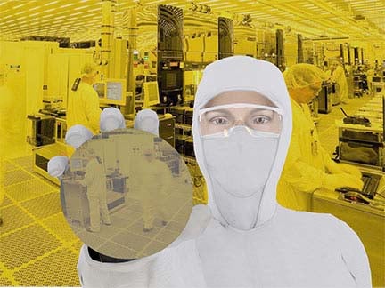
Below is an image of what a plant, such as Intel looks like. Yellow lighting is used for its long wavelength. The lithography processes uses short wavelengths, blue or ultra-violet EUV process. Thus, the yellow long-wavelength light doesn’t interfere with the lithography process.
Current Lithography uses a wavelength of 193 nanometers. EUV uses 13.5 nanometers of light which is more than 10 times smaller than what’s used today. Tinier is “tastier”!
History of Lithography
When semiconductor companies first started to manufacture chips, engineers or technicians drew the chip’s layout on a wall like an elementary school student using a projector to blow up an image to trace for a school project. Then a photo was taken an used to make the chip.
Numerical Aperature, Will it Replace EUV Lithography?
The next evolutionary step to chip making after EUV resides at Intel. Numerical aperature or NA is similar to EUV. It will require a whole redesign of the current processes to make the masks. Numerical aperature (NA) will need a complete overhaul of current semiconductor processing optic system.
It's taken over a decade for EUV to finally hit the market. How long before NA takes over? Impossible to say as the technology is more complicated than the already complicated EUV processes.
