
Why Choose Float Zone (FZ) Silicon Wafers?
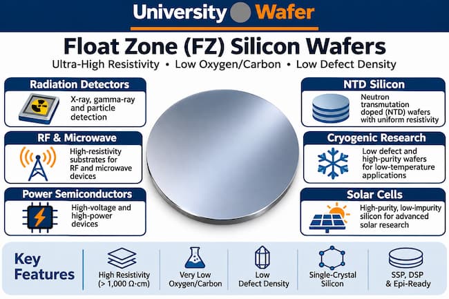
- Ultra-high resistivity up to ~20,000 Ω·cm
- Very low oxygen and carbon levels
- Low defect density for high-performance devices
- Available in 100–200 mm diameters
- N- or P-type, ⟨100⟩ / ⟨111⟩ orientations
- SSP, DSP, and epi-ready finishes
Float Zone Silicon Wafer Applications
Researchers and manufacturers choose Float Zone silicon wafers when low impurity concentration, high carrier lifetime, high resistivity, and low electrical loss are important. Common applications include:
- High-voltage power devices, IGBTs, thyristors, rectifiers, and power semiconductor research
- RF and microwave circuits requiring low substrate loss and high resistivity
- Radiation detectors, X-ray detectors, particle detectors, and high-energy physics instrumentation
- Cryogenic and low-temperature physics, quantum-device research, and low-noise electronics
- Long-lifetime, low-defect semiconductor device development and high-efficiency solar cell research
Looking for float zone silicon with tight specs? Let us tailor a solution.
Get Your Quote FAST! Or, Buy Online and Start Researching Today!
What Are Float Zone Silicon Wafers Used For?
Float Zone silicon is selected for applications where very high resistivity, low oxygen content, high carrier lifetime, and low defect density can improve electrical or detector performance. Because the crystal is grown without direct contact with a quartz crucible, FZ silicon generally contains much less oxygen than standard CZ material.
The Float Zone process uses localized heating to create and move a molten zone along a vertical silicon rod. As the molten region travels, impurities preferentially remain in the melt, helping produce highly purified single-crystal silicon. This makes FZ material especially useful for high-resistivity silicon wafers, detector-grade substrates, RF devices, power electronics, and advanced research.
Float Zone (FZ) silicon wafers are commonly used for the following:
 |
Discrete power |
|---|---|
 |
MOS Power |
 |
High Efficiency Solar Cells |
 |
RF/Wireless Chips |
Intrinsic and Undoped Float Zone Silicon Wafers
UniversityWafer offers a broad selection of intrinsic and undoped Float Zone silicon wafers in research and production sizes, including diced pieces and custom specifications. Available inventory spans multiple diameters, orientations, thicknesses, resistivity ranges, and surface finishes.
| Item | Dia(mm) | Typ/Dop | Ori | Thck(μm) | Pol | Res Ωcm | Specs |
| B119 | 8" | Intrinsic | [100] | 725 | P/E | FZ >20,000 | SEMI notch Prime, Empak cst, TTV<8μm, Bow<10μm, Warp<20μm |
| 7119 | 8" | Intrinsic | [100] | 725 | P/E | FZ >10,000 | SEMI notch Prime, Empak cst, TTV<10μm, Bow<15μm, Warp<30μm |
| 7116 | 6" | Intrinsic | [100] | 675 | P/P | FZ >65,000 | SEMI notch Prime, Empak cst |
| 7117 | 6" | Intrinsic | [111] ±0.5° | 875 | P/P | FZ >10,000 | SEMI Prime, 1Flat (57.5mm), Empak cst |
| I299 | 6" | Intrinsic | [100] | 650 | P/P | FZ >10,000 | SEMI Prime, 1Flat (57.5mm), Empak cst |
| C233 | 6" | Intrinsic | [111] ±0.5° | 675 | P/P | FZ >10,000 | SEMI Prime, 1Flat (57.5mm), Empak cst |
| D233 | 6" | Intrinsic | [111] ±0.5° | 875 | P/P | FZ >10,000 | SEMI Prime, 1Flat (57.5mm), Empak cst |
| J299 | 6" | Intrinsic | [100] | 650 | P/P | FZ >10,000 | SEMI Prime, 1Flat (57.5mm), Empak cst |
| J816 | 6" | Intrinsic | [100] | 1,000 | P/P | FZ >10,000 | SEMI notch Prime, Empak cst, Lifetime > 1,400μs |
| N526 | 6" | Intrinsic | [100] ±05° | 720 | P/P | FZ >10,000 | SEMI Prime, 1Flat (57.5mm), Empak cst, TTV<5μm, With Lasermark |
| O749 | 4" | Intrinsic | [111] ±0.5° | 500 | P/P | FZ >25,000 | SEMI Test, 1Flat, Empak cst, Scratches on both sides |
| P749 | 4" | Intrinsic | [111] ±0.5° | 500 | P/P | FZ >25,000 | SEMI Test, 1Flat, Empak cst, Scratches on both sides |
| F736 | 4" | Intrinsic | [111] ±0.1° | 525 | P/E | FZ >22,000 | SEMI Prime, 1Flat, Empak cst |
| E108 | 4" | Intrinsic | [111] ±0.5° | 500 | P/P | FZ >22,000 | SEMI Prime, 1Flat, Empak cst |
| 7023 | 4" | Intrinsic | [100] | 525 | P/E | FZ >20,000 | SEMI, 1Flat, Empak cst, TTV<5μm, Acid-Etched |
| I693 | 4" | Intrinsic | [100] | 500 | P/P | FZ >20,000 | SEMI Test, 1Flat, TTV<3μm, Scratches on both sides, Empak cst |
| R698 | 4" | Intrinsic | [111] ±0.5° | 500 | P/E | FZ >20,000 | SEMI Prime, 1Flat, Empak cst, Extra 3 free non-prime wafers included with 4 prime wafers |
| D545 | 4" | Intrinsic | [100] | 790 ±2.5 | P/P | FZ >20,000 | SEMI Prime, 1Flat, TTV<2μm, Empak cst |
| H706 | 4" | Intrinsic | [100] | 500 | P/P | FZ >20,000 | SEMI Prime, 1Flat, TTV<3μm, Empak cst |
| 6842 | 4" | Intrinsic | [100] | 525 | P/E | FZ >20,000 | SEMI Prime, 1Flat, Empak cst, TTV<8μm |
| T842 | 4" | Intrinsic | [100] | 525 | P/E | FZ >20,000 | SEMI Test, Flat, Empak cst, TTV<8μm, Unsealed |
| 6993 | 4" | Intrinsic | [100] | 525 | P/E | FZ >20,000 | SEMI, 1Flat, Empak cst, TTV<5μm, Lifetime>1,000μs |
| 6981 | 4" | Intrinsic | [100] | 300 | P/P | FZ >20,000 | SEMI Prime, 1Flat, Empak cst, TTV<5μm, Cassettes of 12 + 2 wafers |
| 6847 | 4" | Intrinsic | [100] | 1,000 | P/P | FZ >20,000 | SEMI Prime, 1Flat, Empak cst |
| L847 | 4" | Intrinsic | [100] | 1,000 | P/P | FZ >20,000 | SEMI Prime, 1Flat, Empak cst |
| 7232 | 4" | Intrinsic | [100] | 525 | P/P | FZ >20,000 | SEMI Prime, 1Flat, Empak cst, TTV<8μm, Bow/Warp<25μm |
| D279 | 4" | Intrinsic | [100] | 640 ±10 | C/C | FZ >20,000 | SEMI Test, 1Flat, Empak cst, As-Cut, Edge-Rounded, EDGE CHIPS, cannot be polished |
| 7327 | 4" | Intrinsic | [100] | 525 | P/E | FZ >20,000 | SEMI Prime, 1Flat, Lifetime>1,000μs, Empak cst |
| F327 | 4" | Intrinsic | [100] | 525 | P/E | FZ >20,000 | SEMI Test, 1Flat, Empak cst, TTV greater than 10μm |
| M376 | 4" | Intrinsic | [111] ±0.5° | 500 | P/P | FZ >20,000 | SEMI Prime, 1Flat, Empak cst |
| D269 | 4" | Intrinsic | [100] | 300 ±10 | P/P | FZ >20,000 | SEMI Prime, 1Flat, Empak cst, TTV<5μm |
| E269 | 4" | Intrinsic | [100] | 280 | P/P | FZ >20,000 | SEMI Prime, 1Flat, Empak cst, TTV<5μm |
| F422 | 4" | Intrinsic | [100] | 3,000 ±50 | P/P | FZ >20,000 | SEMI Prime, 1Flat, Individual cst |
| I218 | 4" | Intrinsic | [100] | 500 | P/P | FZ >20,000 | SEMI Prime, 1Flat, Empak cst, TTV<1μm |
| 7218 | 4" | Intrinsic | [100] | 500 | P/P | FZ >20,000 | SEMI Prime, 1Flat, Empak cst, TTV<5μm |
| 7362 | 4" | Intrinsic | [100] | 525 | P/E | FZ >20,000 | SEMI Prime, 1Flat, Empak cst, TTV<5μm |
| G444 | 4" | Intrinsic | [100] | 300 | P/E | FZ 16,000-20,000 | SEMI Prime, 1Flat, Empak cst, Back-side polish is imperfect |
| D866 | 4" | Intrinsic | [111] ±0.5° | 300 | P/P | FZ 15,000-20,000 | SEMI Prime, 2Flats |
| E775 | 4" | Intrinsic | [100] | 615 ±10 | C/C | FZ >10,000 | SEMI Prime, 1Flat, Empak cst |
| 6878 | 4" | Intrinsic | [111] ±0.5° | 525 | P/E | FZ >10,000 | SEMI Prime, 1Flat, Empak cst, TTV<5μm, MCC Lifetime>1,000μs |
| 7186 | 4" | Intrinsic | [110] ±0.5° | 500 | P/E | FZ >10,000 | Prime, 2Flats, Empak cst |
| 7295 | 4" | Intrinsic | [100] | 500 | P/E | FZ 5,000-10,000 | SEMI Prime, 1Flat, Empak cst, Lifetime>1,000μs |
| F356 | 4" | Intrinsic | [100] | 500 | P/P | FZ >20,000 | SEMI Prime, 1Flat, Empak cst, TTV<0.5μm |
| F982 | 4" | Intrinsic | [100] | 500 | P/P | FZ >20,000 | SEMI Prime, 1Flat, Empak cst |
| G901 | 4" | Intrinsic | [100] | 275 | P/P | FZ >20,000 | SEMI Prime, 1Flat, Empak cst |
| K082 | 4" | Intrinsic | [100] | 500 | P/P | FZ >20,000 | SEMI Prime, 1Flat, Empak cst, TTV<5μm |
| K278 | 4" | Intrinsic | [100] | 3,000 ±50 | P/P | FZ >20,000 | SEMI Prime, 1Flat, Individual cst |
| L801 | 4" | Intrinsic | [100] | 375 | P/P | FZ >20,000 | SEMI Prime, 1Flat, Empak cst, TTV<5μm |
| M847 | 4" | Intrinsic | [100] | 1,000 | P/P | FZ >20,000 | SEMI Prime, 1Flat, Empak cst |
| W981 | 4" | Intrinsic | [100] | 275 | P/P | FZ >20,000 | SEMI Prime, 1Flat, Empak cst, TTV<5μm |
Neutron Transmutation Doping (NTD) of Float Zone Silicon
Float Zone ingots can be supplied as intrinsic material or intentionally doped. One important approach is Neutron Transmutation Doping (NTD), which is used to create highly uniform n-type phosphorus doping in high-purity FZ silicon.
NTD processing is especially valuable when researchers need very uniform resistivity throughout the crystal. Applications include high-voltage power electronics, IGBTs, thyristors, detector-grade silicon, particle physics, and other devices where electrical uniformity is critical.
Float Zone Silicon vs. Czochralski Silicon
Float Zone (FZ) silicon and Czochralski (CZ) silicon are both single-crystal silicon materials, but the growth methods produce different impurity profiles. CZ growth uses a quartz crucible and typically introduces more oxygen into the crystal, while Float Zone growth avoids crucible contact and is preferred when very low oxygen and high purity are required.
For many mainstream integrated-circuit applications, CZ silicon is practical and widely available. FZ silicon is often preferred for high-resistivity devices, RF substrates, radiation detectors, high-voltage devices, low-temperature research, and applications where carrier lifetime or impurity concentration strongly affects performance.
High-Resistivity Float Zone Silicon
High-resistivity FZ silicon wafers can reach resistivity values well above those commonly used in standard semiconductor processing. The inventory on this page includes material above 10,000, 20,000, and even 65,000 Ω·cm. High resistivity helps reduce parasitic conduction and substrate losses, which is useful in RF, microwave, detector, and high-voltage applications.
Researchers working on low-loss electronics may also compare FZ material with our high-resistivity silicon wafers and SOI wafers depending on the device architecture and isolation requirements.
Float Zone Silicon for Radiation and Particle Detectors
Detector applications often require high-purity silicon with long carrier lifetime and low defect density. These properties can improve charge collection and reduce unwanted trapping, making detector-grade Float Zone silicon useful for radiation detection, X-ray instrumentation, nuclear physics, and particle detector research.
High-resistivity FZ material is also used in specialized sensor structures where depletion depth, leakage current, and bulk purity are important design considerations.
Float Zone Silicon for RF and Microwave Devices
RF and microwave silicon substrates benefit from high resistivity because lower substrate conductivity can reduce RF losses and unwanted coupling. FZ silicon is therefore used in wireless-device research, high-frequency circuits, passive components, antennas, resonators, and microwave characterization.
For projects requiring additional electrical isolation, researchers may also evaluate silicon-on-insulator wafers alongside high-resistivity FZ substrates.
How to Choose a Float Zone Silicon Wafer
When selecting an FZ wafer, consider the diameter, resistivity, conductivity type, crystal orientation, thickness, surface finish, total thickness variation (TTV), lifetime, bow, warp, and grade. The best specification depends on the intended device or experiment.
- Resistivity: choose higher values for low-loss RF, detectors, and high-voltage research.
- Orientation: common options include (100), (110), and (111), depending on processing and device requirements.
- Surface finish: SSP, DSP, polished/etched, and epi-ready options may be available.
- Thickness and TTV: important for mechanical handling, wafer bonding, lithography, and precision process control.
- Lifetime: long minority-carrier lifetime can be important for detectors and high-performance devices.