
We would like to grow graphene on nickel foil and would like to know if multilayer graphene films can be produced and transferred onto our own substrates.
Why Grow Graphene on Nickel Foil?
Graphene grown on nickel foil is widely studied for CVD graphene growth, few-layer and multilayer graphene, graphene transfer, sensors, electronic materials, energy-storage research, and other nanomaterial applications. Nickel is an effective catalytic substrate for chemical vapor deposition (CVD) because hydrocarbons can decompose on its surface while carbon can also dissolve into nickel at elevated temperatures.
During cooling, dissolved carbon can segregate or precipitate toward the nickel surface and contribute to graphene formation. Because nickel has substantially higher carbon solubility than copper, few-layer and multilayer graphene regions are more readily produced on nickel. The final graphene structure depends on factors including carbon exposure, growth temperature, nickel thickness and microstructure, surface condition, and cooling rate.
Can Multilayer Graphene Be Grown on Nickel?
A research client asked:
UniversityWafer Response:
Nickel is commonly investigated for producing few-layer and multilayer graphene because carbon can dissolve into the metal during high-temperature processing and subsequently segregate or precipitate toward the surface during cooling. Graphene layer number and uniformity depend strongly on the CVD conditions and catalyst properties.
When a particular layer count is required, another approach is to transfer and stack separately grown graphene films. Graphene may also be transferred onto compatible customer-supplied substrates depending on the required dimensions, substrate material, and transfer specifications.
Get Your Graphene Quote FAST!
Or, Buy Wafers Online
and Start Researching Today!
CVD Graphene Growth and Transfer
CVD graphene is produced by exposing a catalytic growth substrate to a carbon-containing precursor at elevated temperature under controlled conditions. For nickel-catalyzed growth, hydrocarbon decomposition at the surface and carbon uptake into the nickel can both influence graphene formation. Subsequent thermal processing and cooling strongly affect the resulting graphene coverage and layer distribution.
For applications that require graphene on a different material, the graphene can be transferred from the growth catalyst to a target substrate. Polymer-assisted wet transfer, often using PMMA as a temporary support layer, is one commonly used research method. Transfer quality is important because wrinkles, cracks, residues, and contamination can influence graphene's electrical and structural properties.
Depending on project requirements, graphene may be transferred onto silicon wafers , sapphire substrates , quartz , fused silica , glass , flexible polymers, or other compatible substrates.
Nickel vs. Copper for CVD Graphene Growth
Nickel and copper are two important catalytic substrates for CVD graphene, but their different interactions with carbon lead to different growth behavior.
- Nickel foil: Nickel has relatively high carbon solubility. Carbon dissolution followed by segregation or precipitation during cooling can contribute to few-layer and multilayer graphene formation.
- Copper foil: Copper has very low carbon solubility, so graphene growth is predominantly surface-mediated. Under suitable conditions, this makes copper especially useful for monolayer-dominant, large-area graphene growth.
- Process control: Growth temperature, carbon precursor exposure, pressure, cooling rate, catalyst thickness, grain structure, and surface condition can influence graphene coverage, layer number, and defect structure.
What Can Graphene Grown on Nickel Be Used For?
After growth and transfer to an appropriate substrate, graphene produced using nickel catalysts can be investigated for a wide range of research applications. The suitability of a graphene film for a particular device depends on its layer number, defect structure, grain size, contamination level, electrical properties, and the target substrate.
- Electronic devices – graphene transistors, conductive structures, and experimental electronic devices
- Sensors – chemical, gas, biological, and environmental sensing research
- Flexible electronics – conductive films and mechanically flexible device structures
- Energy storage – graphene-based electrodes, batteries, and supercapacitor research
- Photonics and optoelectronics – photodetectors, optical modulators, and related experimental devices
- Composite materials – conductive, thermal-management, mechanically reinforced, and EMI-shielding composites
Graphene Strength and Composite Research
Graphene has exceptional intrinsic mechanical properties, but those properties should not be interpreted to mean that a single graphene sheet can function as macroscopic protective armor. A monolayer of graphene is approximately 0.34 nm thick, so practical structural materials require very different architectures and substantially greater material thickness.
For mechanical and protective-material research, graphene and graphene-derived materials are more commonly investigated as components of polymer, ceramic, fiber, or other composite systems. Their performance depends on graphene loading, dispersion, interfaces, processing, and the properties of the surrounding matrix.

Graphene Grown on Nickel Foil
Graphene grown on nickel foil can be synthesized by chemical vapor deposition (CVD). Nickel acts as a catalytic growth surface for the decomposition of carbon-containing precursor gases and can also dissolve a significant amount of carbon at elevated temperatures. During cooling, carbon can segregate or precipitate toward the nickel surface and contribute to graphene formation.
Compared with copper, nickel has substantially higher carbon solubility. As a result, CVD graphene on nickel foil can form few-layer or multilayer regions, although the final layer distribution depends strongly on growth conditions, nickel thickness and microstructure, carbon exposure, and cooling rate. These characteristics make nickel useful for research involving graphene growth mechanisms, multilayer films, transfer processes, electronic materials, sensors, and other carbon-based nanomaterials.
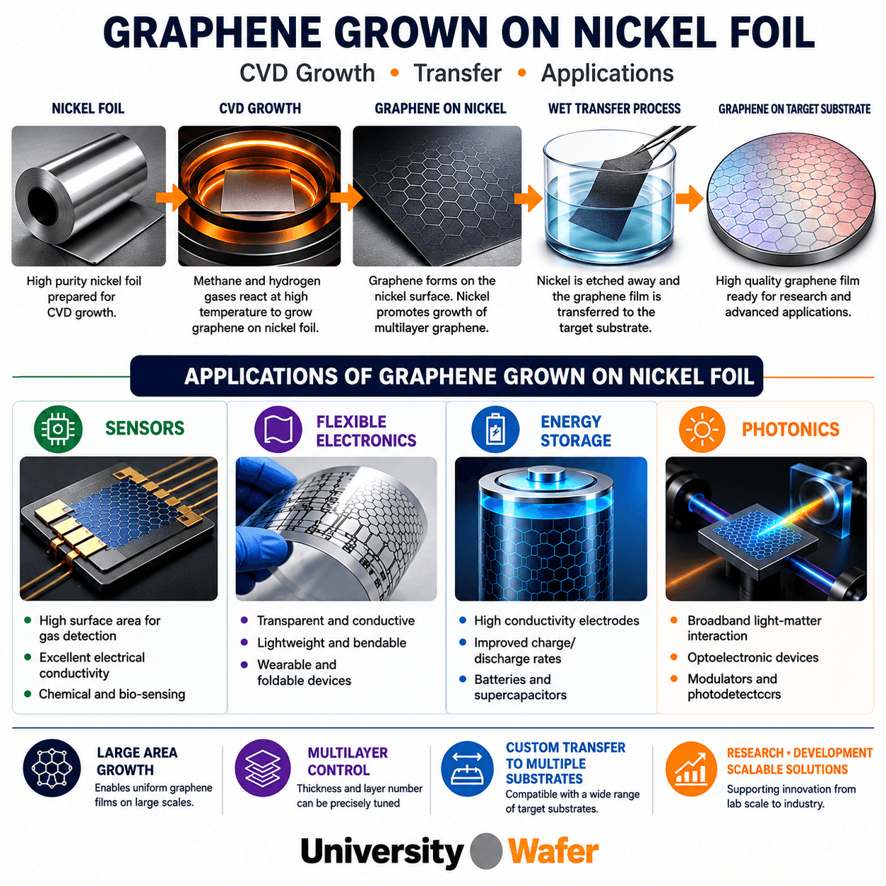
How CVD Graphene Is Grown on Nickel
During CVD growth, nickel foil is typically heated in a controlled reaction environment and exposed to a carbon-containing precursor such as methane. Hydrogen and an inert carrier gas may also be used depending on the process. At elevated temperature, the hydrocarbon decomposes on the catalytic nickel surface and carbon can dissolve into the metal.
As the nickel cools, dissolved carbon can segregate or precipitate toward the surface and contribute to graphene formation. Surface-mediated reactions may also contribute to growth. Because carbon uptake and redistribution are sensitive to processing conditions, controlling the thermal cycle is particularly important when growing graphene on nickel.
Important process variables include:
- Growth and annealing temperature
- Heating and cooling rate
- Carbon precursor concentration and exposure time
- Hydrogen and carrier-gas flow
- Growth pressure
- Nickel foil thickness and purity
- Nickel grain structure and crystallographic orientation
- Surface roughness and cleanliness
Controlling these parameters can influence graphene coverage, layer-number uniformity, grain structure, defect concentration, and electrical properties.
Nickel vs. Copper for CVD Graphene Growth
Nickel and copper are widely studied catalytic substrates for CVD graphene synthesis, but their different carbon solubilities lead to important differences in growth behavior.
| Property | Nickel Foil | Copper Foil |
|---|---|---|
| Carbon Solubility | Relatively high | Very low |
| Common Film Result | Few-layer or multilayer regions are common | Monolayer-dominant growth is commonly achievable |
| Important Growth Behavior | Carbon dissolution, segregation/precipitation, and surface reactions | Predominantly surface-mediated growth |
| Common Research Use | Few-layer/multilayer graphene and growth-mechanism studies | Large-area monolayer graphene research |
Copper is commonly selected when monolayer-dominant graphene coverage is the primary objective. Nickel can be advantageous when researchers want to investigate carbon dissolution and segregation, few-layer or multilayer graphene formation, or the effects of catalyst microstructure on graphene growth.
Why Use Nickel Foil for Graphene Growth?
Nickel provides several useful characteristics as a catalytic substrate for graphene synthesis and research:
- High catalytic activity for hydrocarbon decomposition
- Higher carbon solubility than copper
- Suitable for studying few-layer and multilayer graphene growth
- Compatible with scalable CVD processing
- Available as thin foil for convenient handling and transfer experiments
- Supports studies of carbon segregation and precipitation during cooling
- Can be removed after growth to transfer graphene to another substrate
- Useful for studying catalyst grain structure, surface preparation, and graphene nucleation
Transferring Graphene from Nickel to Another Substrate
For many device and materials applications, graphene must be transferred from the nickel growth catalyst to a target substrate. A common approach applies a temporary polymer support layer, such as polymethyl methacrylate (PMMA), before chemically etching the nickel. The supported graphene film can then be placed onto the target substrate, followed by removal of the polymer support.
Transfer conditions are important because wrinkles, cracks, polymer residue, trapped contamination, and mechanical damage can affect the electrical and structural properties of the transferred graphene.
Potential target substrates include:
- Silicon wafers
- Silicon wafers with SiO₂ surfaces
- Quartz substrates
- Sapphire substrates
- Glass substrates
- Flexible polymer substrates
- Ceramic substrates
- Customer-supplied substrates
Characterization of Graphene Grown on Nickel
Graphene films can be characterized before or after transfer to evaluate their structure, morphology, composition, and electrical behavior. Combining multiple characterization techniques generally provides a more complete assessment than relying on a single measurement.
- Raman spectroscopy – evaluates characteristic graphene Raman bands and can provide information about disorder, layer structure, strain, and doping
- Atomic Force Microscopy (AFM) – examines surface morphology, wrinkles, residues, and step heights
- Scanning Electron Microscopy (SEM) – images surface morphology, coverage, and structural features
- Transmission Electron Microscopy (TEM) – provides high-resolution structural information
- X-ray Photoelectron Spectroscopy (XPS) – analyzes surface chemistry and elemental composition
- Sheet resistance measurements – evaluate electrical transport across the graphene film
- Optical microscopy – provides rapid inspection of transferred graphene, particularly on substrates that provide useful optical contrast
Raman spectroscopy is particularly valuable for graphene because the D, G, and 2D Raman features provide information about defects or disorder, graphene structure, strain, doping, and layer-dependent behavior. Raman results should be interpreted together with the substrate, excitation wavelength, and other characterization data.
Applications of Graphene Grown on Nickel Foil
After growth and, when required, transfer to an appropriate substrate, graphene produced using nickel catalysts can be investigated for a wide range of electronic, sensing, energy, photonic, and materials applications.
Electronic and Flexible Devices
Graphene's electrical conductivity, mechanical flexibility, and two-dimensional structure make it useful for research involving graphene transistors, flexible electronics, conductive films, and wearable devices. Device performance depends strongly on graphene quality, layer number, transfer cleanliness, substrate selection, and device architecture.
Sensors and Biosensors
Graphene's high surface-to-volume ratio and sensitivity to changes in its local electronic environment make it attractive for research involving chemical sensors, gas sensors, and biosensors. Surface functionalization can be used to provide selectivity toward particular molecules or biological targets.
Energy Storage and Electrochemical Research
Graphene and graphene-based composites are investigated as conductive and high-surface-area materials for batteries, supercapacitors, electrodes, and electrochemical systems. Their performance depends on factors including graphene morphology, defect structure, layer stacking, surface chemistry, and integration with other active materials.
Optoelectronics and Photonics
Graphene's broadband optical response and electrically tunable properties have led to research involving photodetectors, optical modulators, transparent conductive structures, and other photonic and optoelectronic devices.
Composite and Functional Materials
Graphene can also be incorporated into polymers, ceramics, and other material systems to investigate improvements in electrical conductivity, thermal transport, mechanical reinforcement, and electromagnetic-interference shielding.
Graphene Films and Custom Transfer Services
UniversityWafer provides graphene films and substrates for universities, government laboratories, and industrial research. Graphene can be transferred to selected target substrates depending on available specifications and project requirements.
When requesting a quote, provide the desired graphene configuration, target substrate material, substrate dimensions, quantity, and any relevant surface or transfer requirements. Providing detailed specifications helps determine the most appropriate material and processing options for your research.