
Gallium Arsenide for Heterojunction Bipolar Transistors
We can customize your specs to create (HBT). Below is a recently quoted spec. Please let us know what specs and quantity we can quote for you!
Item Qty. Description
FM91b. 1 Substrate: GaAs 3ӯ
Epi layer 1: 500 nm AlGaAs sacrificial layer
Epi layer 2: 10 nm undoped, lattice matched InGaP
Epi layer 3a: 60 nm lattice matched InGaAsP barrier
Epi layer 3b: 5 nm compressively strained InGaP QW with PL around 670 nm
Epi layer 3c: 10 nm lattice matched InGaAsP barrier
Epi layer 3d: 5 nm compressively strained InGaP QW with PL around 670 nm
Epi layer 3e: 10 nm lattice matched InGaAsP barrier
Epi layer 3f: 5 nm compressively strained InGaP QW with PL around 670 nm
Epi layer 3g: 60 nm lattice matched InGaAsP barrier
Epi layer 4: 10 nm undoped, lattice matched InGaP
Epi layer 5: 100 nm AlGaAs cap
Get Your Quote FAST! Or, Buy Online and Start Researching Today!
Related III-V and Semiconductor Substrate Resources
- Gallium arsenide (GaAs) wafers for HBT devices
- AlGaN and compound semiconductor substrates
- III-V semiconductor substrates for RF and optoelectronics
- Epitaxial wafers for advanced device fabrication
- Silicon wafers for semiconductor applications
- Optoelectronic substrates and materials
- Semiconductor fabrication process
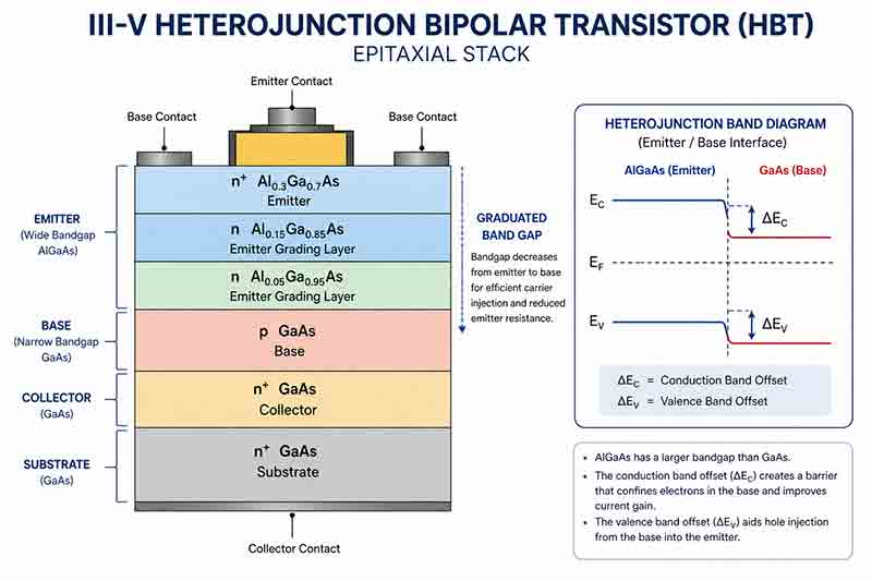
Heterojunction Bipolar Transistor (HBT)
Heterojunction bipolar transistors (HBT) are a type of bipolar transistor where the emitter transition usually assumes a heterojunction structure, i.e. a broadband gap material in the emitter region and a narrow band are used - gap materials are used for the base region. They form the basis for the use of different semiconductor materials for both the emission and collector basis. The bipolar heter-mojunction transistor, or H BT, has attracted a lot of attention due to its ability to use very fast devices and is one of the most promising technologies for use in electronic devices. [Sources: 0, 1, 3, 5]
Since bipolar transistors have a material structure, they can produce an inverse distortion of the collector transition. The premise is that the bipolar transistor is not damaged and the current gain can be reduced without damaging the transistor. When analyzing and designing bipolar transistor circuits, it should be noted that the reverse bias of the HBT (or of any other heterojunction transistor) cannot be exceeded. The reverse distortions must not be too great, otherwise the currents are too high and the current gains too low, which will damage the transistor. [Sources: 1]
If the emitter connection of a bipolar transistor has a reverse bias that exceeds the permitted range but does not limit the current flow through the transistor, an avalanche can occur without damaging the device. If the holes do not start to leak out of the base, the saturation voltage will be lower than that of homojunction bipolar transistors and the voltage will be applied to both base and emitter. [Sources: 1, 5]
To improve integration density, an I2-L gate was proposed for use in heterojunction transistors. This invention is directed against the energy band of heterojunctions, which is influenced by the choice of material itself. It is generally related to the fact that such heterjunction transitors have a graduated band gap region, which can lie between the emitter base and the collector. [Sources: 2, 3, 5]
If the two PN transitions of a bipolar transistor are forward-biased, the transistor is in the cut-off region and not within the saturation region. However, if the bipolar transistors are biased backwards (forward - biased), the transistors are also outside the saturation range, and the exact opposite is true in saturation ranges. [Sources: 1]
If the bias voltages mentioned above are exchanged, the bipolar transistors work in both cut-off and saturation ranges. [Sources: 1]
In analog devices, the parameters of the bipolar transistor are influenced by the parameter of bipolar transistors, but to varying degrees. These parameters can take into account the Tiwari effect [11] and the soft knee - observed in the case of ISB - NB, which are taken into account by a thermal equivalent circuit modelled on the thermal evolutionary equation, as shown in the AgilentHBT model [12]. As the "soft knee" serves as the basis for the calculation of the ISBs and NB, we can use the same parameters as the analog device, such as temperature, voltage, saturation and cut-off. [Sources: 1, 4]
The electric symbol of the NPN bipolar transistor is shown on the right and the base beam transition and collector transition are in a forward biased state, while the base collector collection point is in a backward biased state. In the symbol of the bipolar transistors, the arrow at the "base" or "emitter" points in the direction of current. The arrow in "base" (the sender) points to the radiators, and in "collector" the arrows at the base and the radiators point to the currents. As a result, their voltage is lower than that of bipolar transistors, which allows the calculation of their output voltages and interruptions in an analog device. [Sources: 1, 3]
Therefore, the bipolar transistors must be distinguished from the NPN transistor with its two PN transitions and its inverse bias voltages. Since bipolar transistors have two PN transistors, their reverse bias voltage may be sufficient to prevent a reverse breakdown of the P-N transition. [Sources: 1]
A bipolar transistor consists of three different doped semiconductor regions, which are defined as upper, lower and collector-specific regions of the bipolar transistor PNP. The common collector region is integrated into the lower region, whereby the transistor works as an emitter of the upper type. A bipolar transistor consists of a single PN transistor with three doping semiconductors, each of which is responsible for one of its two transitions and its inverse bias voltage. In addition to the two doping regions (top and bottom), a P-NPipolar transistor also consists of a second doping region (bottom) with its inverse bias voltage and the inverse - bias voltage. [Sources: 1, 3]
As mentioned above, the heterojunction bipolar transistor, which has two transistors, one for the conductor band and one for the transceiver band, is described as a PNP transistor. It should be understood that this invention could not be realized because the valence bands would have been aligned and there would have been no difference in the conduction bands. If the base of the polar transistor collector is considered as an input, a two-port network can be analyzed with Thevenin's theorem. [Sources: 1, 5]
Sources:
[0]: https://www.nrl.navy.mil/estd/branches/6870/6876/HBT
[2]: https://www.google.com.na/patents/US4794440
[3]: https://www.google.com/patents/US5329145
[5]: https://www.google.com.gi/patents/US4821082