
HOPG Sizes and Custom Research Pieces
A scientist developing a UHV experiment asked about HOPG pieces approximately 5.5 × 5.5 × 0.5 mm and whether the material could be reduced to size. The inquiry described an intended getter application; it does not establish a general gas-sorption specification for HOPG.
The response listed the following dimension options. The 5.5 mm square example has a different thickness from the original request.
| Length × width | Thickness |
|---|---|
| 5.5 × 5.5 mm | 1.0 mm |
| 10 × 10 mm | 0.5 mm |
| 10 × 10 mm | 1.0 mm |
| 20 × 20 mm | 1–2 mm |
| 30 × 30 mm | 1.5–2 mm |
A separate order on the original page listed ten pieces of 10 × 10 × 0.5 mm HOPG. Confirm current dimensions, grade, tolerances, availability, and lead time with your quote.
Cleaving can expose a fresh graphite surface, but accurate lateral dimensions should be specified when ordering rather than relying on manual breaking or shaving.
Get Your Quote Fast! Send your HOPG specifications below, or browse research substrates online and start researching today.
What to Include in Your HOPG Inquiry
- HOPG dimensions and thickness, including tolerances
- Required grade or mosaic spread
- Working-face and cleaving and surface-preparation requirements
- Purity or characterization documentation
- Mounting constraints, intended application, and quantity
What Is Highly Oriented Pyrolytic Graphite?
HOPG, also called highly ordered pyrolytic graphite, is synthetic graphite with closely aligned crystallites. Carbon atoms form strongly bonded sheets, while weaker interactions between sheets allow the material to cleave along the layers. HOPG is an oriented graphite material rather than a metal, an amorphous carbon film, or a single graphene sheet.
A freshly cleaved HOPG basal plane can provide flat terraces separated by steps. This combination of a renewable surface and electrical conductivity makes HOPG useful for surface imaging and experiments involving deposited molecules, nanoparticles, and other nanoscale structures.
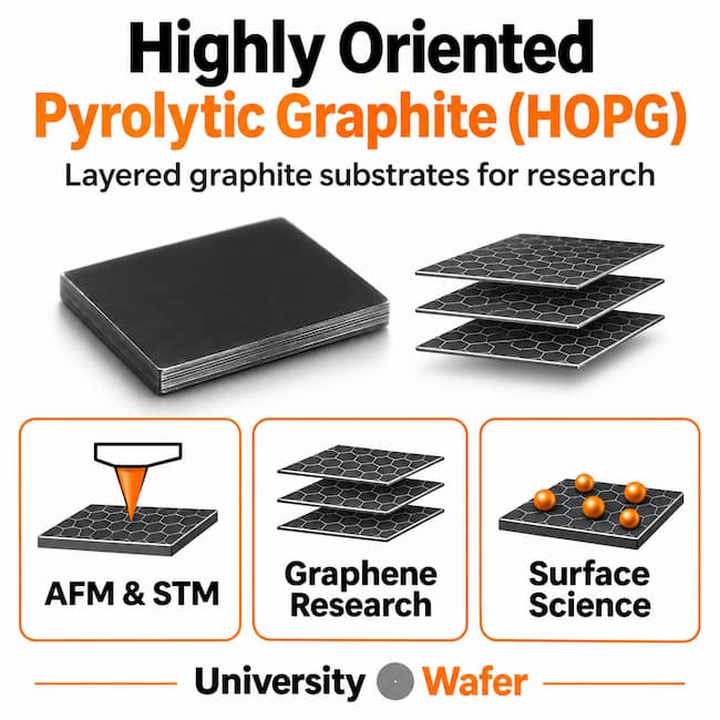
HOPG Substrates for AFM and STM
Atomic force microscopy (AFM) uses HOPG as a substrate for studying surface topography and deposited specimens. Terraces, steps, and adsorbed material influence the observed surface. Select a grade and preparation method that provide suitable working areas for your scan size.
In STM and atomic-scale surface research, HOPG provides an electrically conductive layered carbon surface. It is widely used as a reference specimen for atomic-resolution imaging. STM contrast depends on electronic structure and imaging conditions, so bright features should not automatically be interpreted as a direct map of every carbon atom.
HOPG Mosaic Spread and Grade Selection
Mosaic spread describes the angular distribution of crystallite orientations. A smaller value indicates closer alignment. It is a material-selection parameter, not a measure of monolayer graphene thickness or a universal guarantee of surface roughness.
HOPG is offered commercially under grade designations such as ZYA, ZYB, and ZYH. Confirm the actual mosaic-spread specification and measurement convention rather than assuming that a grade label defines every property. Request your preferred grade or angular spread so the available material can be checked.
| Parameter | What to specify |
|---|---|
| Mosaic spread | Target angular spread, tolerance, and any certification requirements. |
| Dimensions | Working area, overall piece dimensions, thickness, and tolerances. |
| Surface | Cleaving requirements, usable face, terrace needs, and preparation constraints. |
| Purity | Required impurity limits and supporting documentation, if needed. |
| Experimental environment | Ambient, liquid, or vacuum conditions; mounting and temperature requirements. |
HOPG vs. Graphene for Exfoliation Research
Graphene is a single layer of carbon atoms; HOPG contains many stacked layers. Mechanical exfoliation can separate thin flakes from graphite, but producing and identifying a monolayer requires additional handling and characterization.
Researchers transferring flakes to a receiving surface may use thermal oxide silicon wafers. The receiving substrate and oxide thickness should match the optical inspection and device requirements. Raman spectroscopy can support characterization of graphitic materials alongside microscopy and other measurements.
Surface Science and Electrochemical Applications
The basal planes, step edges, and defects of HOPG provide different environments for molecular adsorption and surface reactions. Researchers use graphite surfaces to investigate deposited films, molecular assemblies, surface functionalization, and electrochemical interfaces. Surface preparation and exposure history should be controlled when comparing measurements.
In graphite intercalation research, atoms or ions are introduced between carbon layers. This changes the material and should be distinguished from experiments on a freshly cleaved, untreated HOPG surface. The behavior depends on the intercalant and experimental conditions.
HOPG for X-Ray Optics and Thermal Studies
Oriented graphite is used in selected X-ray monochromator and analyzer applications. The required mosaic spread, dimensions, mounting, and diffraction geometry depend on the instrument. See our X-ray diffraction and crystal-characterization guide for background on diffraction measurements. A microscopy substrate should not automatically be treated as a certified X-ray optical component.
Graphite is anisotropic: its electrical and thermal behavior differs parallel and perpendicular to the layers. For thermal measurements, specify the measurement direction, temperature, and material grade. Flexible graphite heat-spreader sheets and bulk HOPG research substrates are different product forms.
How to Cleave and Specify HOPG
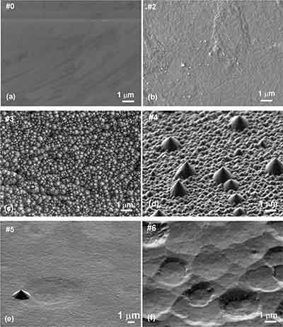
Cleaving removes layers to expose a fresh basal-plane surface. Adhesive-tape cleaving is commonly used, with the method chosen to limit unwanted contamination or damage. For complementary topography measurements, compare silicon substrates for AFM analysis. Each cleavage reduces the remaining thickness, and the resulting surface can contain terraces and steps.
Cleaving parallel to the layers is different from cutting a piece to a precise length and width. Request custom dimensions and edge tolerances when the sample must fit a holder, electrode assembly, or vacuum fixture. Include any adhesive, cleaning, or mounting restrictions in your inquiry.
HOPG Substrate Questions
What is highly oriented pyrolytic graphite (HOPG)?
HOPG is a highly oriented form of synthetic graphite made of stacked carbon layers. It is used as a conductive, cleavable substrate for scanning probe microscopy, graphene exfoliation, and surface science.
What is HOPG used for?
HOPG is used in AFM and STM studies, molecular adsorption experiments, electrochemical surface research, graphene exfoliation, and selected X-ray optics. The required grade and preparation depend on the application.
What does HOPG mosaic spread mean?
Mosaic spread describes the angular distribution of crystallite orientations. A smaller spread indicates closer alignment. Specify the required value and measurement convention with your quote; HOPG grades are not interchangeable.
Can HOPG be cleaved or cut to size?
HOPG can be cleaved parallel to its carbon layers to expose a fresh basal-plane surface. Cleaving does not guarantee an accurate lateral size. Request custom dimensions and tolerances when piece size is critical.
Is HOPG the same as graphene?
No. Graphene is a single carbon layer, while HOPG contains many stacked layers. HOPG can be used as a source for mechanical exfoliation, but an HOPG piece is not itself a monolayer graphene film.
Can I request 10 × 10 mm HOPG substrates?
Yes. The listed size examples include 10 × 10 × 0.5 mm and 10 × 10 × 1.0 mm HOPG pieces. Send your dimensions, grade or mosaic spread, and quantity to confirm current availability and pricing.
Request HOPG substrate pricing and availability with your size, thickness, mosaic spread, and quantity.
Related Carbon Materials and Research Substrates
- AFM substrates and silicon surface analysis
- Surface roughness and substrate selection
- X-ray diffraction and crystal orientation analysis
- Graphene materials and coated substrates
- Scanning tunneling microscopy substrates
- Thermal oxide silicon receiving substrates
- Raman spectroscopy substrates and characterization
- Silicon wafers for materials research
- Sapphire substrates
- Single-crystal quartz substrates
- Fused silica wafers