
The Cleaning of Silicon Wafers
The process of Cleaning Silicon Wafers must be carried out under the strictest conditions, keeping in mind the fact that these delicate components are prone to damage.
UniversityWafer, Inc. subtrates are clean room sealed for quick use. Please let us know what specs work for you or buy online.
Moreover, they are also highly sensitive, making them extremely fragile. Hence, semiconductor manufacturing businesses must follow a specific cleaning protocol to ensure a good quality of finished products. In general, the process of Cleaning Silicon Wafers involves heating an acetone bath to 55degC and soaking the wafer in the solution for about 10 minutes.
Get Your Quote FAST! Or, Buy Online and Start Researching Today!
Why is it Important to Clean Silicon Wafer Surfaces?
The removal of contaminants and particles that may be deposited on the wafer surfaces or maybe leftover after carrying out wafer operations has to be achieved. This has to be done to reduce the chances of defects in the final products that are to be obtained. The unwanted particles or impurities may block the surfaces where etching has to take place in the process undesirable results are inevitable. Also, since the size of the current silicon wafers microstructure is small, the effect if the contaminants or deposited particles also will impact on the diffusion process. In addition to the stated reasons, cleaning the wafers aids in reducing the integrated circuits element dimensions. The final product having been exposed to the stated inhibitors is expected to have reduced reliability, stability, and quality.
Semiconductor Wet Cleaning Process
Wafer cleaning task is one of the most repeatedly carried out procedure that is undertaken when fabricating wafers. With the ever-changing technology and device shrinking property, cleaning processes do get complicated each time. The cleaning process should not only be done to the wafers each time as the machines and equipment’s used also have to be cleaned. Wafer contaminants range from particles with a diameter range of 0.1 to 20 microns, organic and inorganic contaminants, and impurities. Cleaning methods can be categorized as either wet or dry methods. Wet cleaning does involve solvents, acids, or water. Dry cleaning on the other hand uses lasers, aerosols, or ozonated chemistries. The wet silicon wafer cleaning method is the most commonly used way to clean wafers. The dry methods are most suitable for metalized surfaces (Karen Reinhardt, 2008).
Wafer cleaning has to be done without introducing any additional impurities or contaminants to the final surface.
Wet Silicon Wafer Cleaning Methods
With wet cleaning, the surface impurities can be removed without creating rough surfaces afterward. However, after the solvents have been used, they will have to be disposed thus this method generates wastes. Below is a simplified approach that explains the whole process.
Solvent Cleaning
The use of solvents to remove impurities on the surface of the silicon wafer is classified as the most effective. This step is done first in the many subsequent cleaning procedures that have to be done. Organic impurities or oils are particularly effectively eliminated by using this method. The drawback of the solvent cleaning method is that residues of the solvent may be deposited on the wafer surface after cleaning. To counteract this, particular solvents have to be used i.e. methanol and acetone. The two solvents do serve different roles in the cleaning process. One is used to make sure that contaminants have been removed while the other solvent makes sure that the substrate material is returned to its expected state. Two separate ultra-sonic baths have to be made such that one has acetone while the other has got methanol. The bath that has acetone is heated to attain temperatures of fifty-five degrees Celsius after which the wafer to be cleaned has to be sunk in the warm bath. After ten minutes inside the acetone bath, the wafer is dipped inside the second bath that has methanol for five minutes. Lastly, the wafer is rinsed with deionized water then blow-dried using nitrogen.
RCA Cleaning
This process is used to remove organic materials, heavy or alkali metal ions that may be present on the surface of the wafer after the solvent cleaning process. The unwanted particles are removed through ultrasonic agitation. Sulphuric acid and hydrogen peroxide in ratio ranges of between 1:1 to 1:4 is used where the silicon wafer is dipped into such a solution for about ten minutes while the temperature conditions are maintained between one hundred and a hundred and fifty degrees Celsius. The next step involves dipping the wafer into a solution of hydrochloric acid and water mixed in the ratio 1: 10 and the process takes place for one minute. Water is then used to rinse the wafer surface at room temperature conditions. De-ionized water is preferred as compared to ordinary water as it gives the best results (Bera, 2019). The objective of the RCA cleaning process is to oxidize the silicon to provide a thin oxide layer on the wafer surface that will protect the wafer.
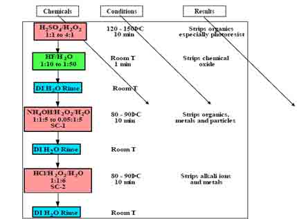
Figure 1: RCA cleaning process. (Bera, 2019)
c. Hydrofluoric Acid Dip
This final stage uses hydrofluoric acid in a glass dip to remove the silicon oxide layer chemically. A solution made up of twenty milliliters of the acid with four hundred and eighty milliliters of water is prepared. Then the resulting wafer is immersed inside for two minutes after which running deionized water rinses the wafer. To verify that the contaminants have been removed, a wettability test is done.
2.Dry cleaning methods of silicon wafers.
Dry silicon wafer cleaning methods are less harmful to the environment as few chemicals are needed. Theoretically, large wafers are better suited to the dry-cleaning process as opposed to smaller ones. This is due to the higher need for more solvents, water, or waste disposal associated with increased size. Despite cost reduction, dry cleaning is also compatible with most of the processes of technology being used currently.
a. Laser cleaning
In this method, a laser is used to eliminate the contaminant from the wafer surface by lifting it. Inert gas is then used to sweep away the impurity from the surface. Through the operation, the surface of the wafer may be surface roughened slightly. The photoresist films, metallic ions, or chemical impurities are also removed in the process.
Future developments in cleaning silicon wafers
It is predicted that wet cleaning processes will still be dominant in the coming future owing to their unquestionable cleaning capability. Despite this, research is being done to find out better methods that will minimize chemical usage when cleaning to address the growing environmental conservation plea by relevant authorities. It is anticipated that dry cleaning strategies will be used to complement the limitations involved as a result of wet cleaning processes.
Semiconductor Cleaning Process
To learn more about the semiconductor cleaning process. Contact us.
References
Bera, B. (2019). Silicon Wafer Cleaning: A Fundamental and Critical Step in Semiconductor Fabrication Process. International Journal of Applied Nanotechnology, 8-13.
Karen Reinhardt, W. K. (2008). Handbook of Silicon Wafer Cleaning Technology Materials Science and Process Technology Series. William Andrew .
What is The Process for Cleaning Silicon Wafers?
The first step of this process is not essential. However, it is necessary to clean the surface of the wafer to extend the life of cleaning solutions. After cleaning, the wafers should be immersed in the preferred film stripping solution. The final step is to rinse the silicon wafers with deionized water. This step is also necessary because it may result in the deposition of residues, and it is also necessary to dry the silicon wafers after cleaning.
The second step of the cleaning process is to apply a solution of hydrofluoric acid.  This solution has an oxidizing effect on the surface of silicon wafers and is best suited for cleans that do not require too much acid concentration. A 20% nitric acid solution is used to remove organic residues. The solution is made of five parts water and two parts hydrogen peroxide. The silicon wafer is immersed in this solution for about six to ten minutes. Once the solution dries, the silicon wafer is rinsed in deionized water.
RCA Clean
The clean is a standard cleaning process for wafers. It must be performed before the high-temperature processing steps. The RCA cleaning is performed by heating the RCA solution to 75 or 80 degrees Celsius for 10 minutes. The RCA clean mixture combines with the metal and changes its zeta potential. This results in a thin layer of silicon dioxide on the surface and metallic contamination on the surface of the silicon wafer, which will be removed in the following step.
The process of Cleaning Silicon Wafers is complicated. The materials are highly fragile and can easily become contaminated. Various processes are employed to clean the silicon wafers. Usually, the three-step procedure is used to remove oxidized residues from the substrate. This method uses a chemical solution with sulfuric acid and hydrogen peroxide to make the surface water compatible. It also removes photoresist films and other impurities.
The process of cleaning Silicon Wafers involves using a deionized water bath. This water is highly acidic and must be free of sulfur and other chemicals. The water is essential for the proper functioning of the oxidized solution. It is used in the oxidizing treatment for silicon wafers. After the slurry is applied, it is rinsed with deionized liquid. The final step is the ozone wash.
Solvents are also used for the cleaning of silicon wafers. They are effective in removing oil, organic particles, and other contaminants from siliRCAcon surfaces. The solvents that are used in this process tend to leave a residue on the silicon surface. So, an alkaline bath is necessary for a proper cleaning of silicon wafers. Aside from ensuring a clean surface, it also removes the impurities.
Silicon Substrate Cleaning Procedure
Wet cleaning is the most popular method for cleaning silicon wafers. It uses caustic solutions to dissolve dirt and  other impurities and allows the wafers to be thoroughly cleaned. Ultrasonic cleaning takes as long as 30 minutes, but it should not be used for very long. If the ultrasonic exposure time is too long, it will damage the crystal lattices. Furthermore, excessive exposure to ultrasonic energy may result in the growth of an oxide layer on the silicon wafer.
The cleaning process is the most important part of semiconductor manufacturing. The cleaning process eliminates any particles and contaminants that might affect the finished product. It also reduces the size of integrated circuit elements. A proper cleaning process will ensure a good clean and reduced-size semiconductor. So, it is vital to ensure a clean and efficient manufacturing environment. It is crucial for the success of semiconductor manufacturing. There are many reasons for the importance of a clean wafer.
University of New South South Wales Silicon Cleaning Video
What is Substrate Cleaning?
Dry substrate cleaning
The process of dry substrate cleaning is one of the most important steps in the photovoltaic industry. It removes the oxide deposit that can prevent the substrate from receiving a proper coating. This process can also be used to remove organic and carbon-based contaminants from the substrate. After the dry cleaning step, the substrate is rinsed with a liquid cleaning solution.
The most common applications of dry substrate cleaning involve photoresist descum and stripping. These processes produce reactive ions and radicals that react with the contaminants present on the surface of the substrate. The removal of these pollutants can improve the quality of the subsequent etching steps. The descum step helps in achieving high sidewall profiles, whereas photoresist stripping is more aggressive.
O2 plasma etching
O2 plasma etching is a method of cleaning non-metallic surfaces. The gas that is most commonly used for plasma cleaning is oxygen. The gas is available in all types of plasma etching systems and is often used to clean non-metallic surfaces. In addition, the use of oxygen increases the surface wettability of non-metallic materials. The picture below shows the relative carbon content of a substrate before and after O2 plasma etching.
Plasma etching is highly repeatable compared to conventional liquid bath etching. It is also very cost-effective. In addition, the process can be done on a variety of materials. Figure 5.19 shows an example of plasma etched substrate. Plasma etching is an effective method for cleaning semiconductor substrates.
Plasma etching removes photoresist from entire surfaces or selected areas. The technique allows users to control the depth of etching and improve bonding in PCBs and semiconductors. The process also reduces oxide buildup on bond pads and creates a more reliable electromechanical connection. Moreover, the material will have improved adhesion and shelf life.
Plasma cleaning is necessary for silver and copper wire bonding. The resulting O2 plasma generates oxygen radicals and atomic oxygen. These gases react with metal surfaces to remove organic contaminants. However, this process also oxidizes the surfaces of the metals. Moreover, oxidized metal surfaces affect the intrinsic brightness and reflectivity of LEDs.
RF glow plate
RF glow plate substrate cleaning is an essential process to ensure the longevity of your instrument. Using special cleaning agents that have been specially formulated for this purpose is crucial to ensure that the surface of your RF glow plate remains as shiny and clear as possible. For this purpose, you can use special mataha (a type of saretaburazuma) to effectively clean your plate's surface.
The benefits of RF glow plate substrate cleaning include reduced energy consumption and lower costs. In addition, RF glow plate processes are suitable for delicate substrates, as they use relatively low levels of energy and therefore don't damage them as much. In comparison, ion source processes are much more powerful than glow plates, and can also be used to achieve higher impact plasma etching. In addition, gridded ion sources are also suitable for etching applications, since they can provide independent control of energy and current over a wide area.
Microwave plasma
Microwave plasma is an effective cleaning method that is both quick and efficient. This plasma cleaning technique can clean even the smallest substrates. Its high cleaning rate makes it ideal for high-volume applications. However, further study of this plasma cleaning method is needed to define appropriate threshold values, explore the interactions between electrons and ions with the magnetic field, and improve cleaning uniformity.
In the present study, a batch-type microwave plasma (B-MW) was used as an alternative to conventional S-RF plasma. It was found that a constant-flow pattern improved the surface wettability and uniformity. In addition, it exhibited improved cleaning performance compared to conventional S-RF plasma. Further, increasing the cleaning time and power resulted in an improved surface wettability.
In addition, we found that the dtreatment rate of the plasma was directly proportional to the power, and the cleaning time was inversely proportional to the sample area. These results are consistent with those found when using microwave to break down a neutral gas. However, we can expect more improvements in cleaning efficiency when using higher flow rates of O2.
The plasma process consists of several minor modifications to the conventional oven. It requires a moving table, a rotating antenna, and supports to position the reaction vessel. These modifications ensure that the microwave energy is focused on the sample. In the microwave plasma oven, samples are prepared in a Pyrex vessel filled with argon. A fire brick is used to position them in the microwave field. The duration of exposure varies from 2.5 to six hours.
Gravel cleaner
Before using a gravel vacuum to clean substrates, it is important to know how to properly use it. Gravel vacuums are designed to clean substrates by pulling dirt, water, and debris from them. While gravel vacuums are less messy than sand, they should be used with caution. The vacuum must be moved gently across the surface of the substrate, so that small pieces of sand and substrate do not escape while cleaning.
A gravel vacuum is one of the most common aquarium cleaning tools. It is able to reach all corners of your tank, including underneath decorations. Another great feature is that it is easy to use. It is a very convenient way to clean the substrates in your aquarium. This makes it easier to remove dirt and debris without having to disassemble them.
Gravel vacuums come in a variety of sizes and designs. The most effective size is the one that is half the height of your tank. It will be easier to reach the substrate with a bigger tube. Another option is to purchase a siphon hose, which can be easily hooked up to a bucket or window.
Gravel vacuum cleaners are convenient for cleaning substrates, and you can use them for several different purposes. For example, the Gravel Cleaner by NICREW is a vacuum cleaner that cleans the gravel and debris in a tank without disturbing the bottom layer of gravel. This device works well with both partial and full water changes. It comes with a plastic scraper to scrape off algae and other contaminants from the substrate. It also features a vacuum head that can be used for quick cleaning and water changing.
Pre-cleaning
Pre-cleaning is an essential step in the process of thin film deposition. It removes contaminants from the substrate and improves adhesion of the deposition layers, thereby ensuring defect-free, high-performance coatings. Several pre-cleaning methods are available, each with different advantages and disadvantages.
In some cases, high-energy pre-cleans can damage sensitive substrates. In these cases, a low-energy, low-density pre-clean may be appropriate. In many cases, the yield of the process can be improved by using low-energy pre-cleans. In other cases, using a high-density ion source may reduce yield without considering surface sensitivity.
The pre-cleaning step may be performed before or after barrier layer deposition. The objective is to reduce contaminants on the barrier layer to increase electromigration resistance. In particular, pre-cleaning is beneficial for barrier/lining layers that are made of tantalum or titanium. In addition, remote plasma can be used to generate H 2 radicals, which may improve adhesion to CVD deposited Al or Cu.
The pre-cleaning step may also involve an etching step. In this step, hydrogen radicals are introduced to the substrate to dissolve native oxides. The remote plasma source preferably delivers a soft etch, not damaging the bottommost sublayer of the feature. If necessary, the substrate is subjected to a second step of reducing native oxides on the substrate.