HRFZ Si Wafers
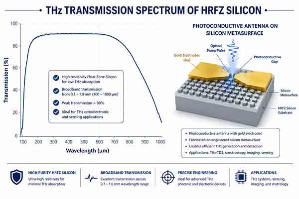
The high resistance traditionally used in THz applications and the thickness of the wafers range from 775 to 12 inches per wafer. Float Zone Silicon (HRFZ Si) is the best studied substance for operation in this area and has the best transmission performance. Optical silicon is generally good for transmission up to 10 microns, but additional pass bands of 30 - 100 microns are suitable for use in high-frequency applications such as glass fibers. Silicon has a pass-through band of 10 - 30 microns, while optical silicon, with its low scattering and high resistance, is best suited for high frequencies in the range of 100 - 300 microns. [Sources: 0, 3, 10]
Get Your Quote FAST! Or, Buy Online and Start Researching today!
Related High-Resistivity and Silicon Wafer Products
- Silicon Wafers
- Float Zone Silicon Wafers
- Silicon-on-Insulator (SOI) Wafers
- Epitaxial Silicon Wafers
- Sapphire Wafers
What are HRFZ Silicon Wafers?
Terahertz radiation (THz), which is located at microwave and infrared frequencies, has closed the gap between electronics and optics and has aroused considerable interest in broadband gas phase spectroscopy. This offers the possibility to observe dust emissions at wavelengths of only 1.5 micrometres and up to 10 micrometres. [Sources: 4, 9]
The Si wafers were calibrated using Fourier Transform Infrared Spectrometers (FTIR), which were used in previous work [6-8]. Using the optical substrate as a reference, the recorded THz waveforms and their Fourier spectra are shown in Fig. 5, co - calibrated to a thickness of 1 micrometer for each layer of the wafer and the same thickness for the other layers. [Sources: 6, 9]

To model the performance of the FPI, five parameters were required for each layer of Si wafers: thickness, layer thickness, temperature, frequency, wavelength and wavelength of light. [Sources: 8]
Although the refractive index of silicon also has a frequency dependence, this effect was modeled as negligible in the measured frequency range compared to the expected measurement accuracy, and the only variable the model matched was the thickness of the photolithographic mask itself. THz waves can be generated with many methods, including photoconducting antennas, where they generate a signal that is pulsed with a THZ signal and becomes a classic "THz resource" for TH-Z spectroscopy. This design scales the near-infrared spectrum to a dimension defined by a sharp lithography mask, with an FPI of 0.5 and a wavelength of 10 nm. [Sources: 2, 5, 8]
Silicon is a powerful, cost-effective and highly efficient optical material for optical spectroscopy. Honour Optics manufactures and houses a wide range of high-performance spherical and aspherical infrared infrared silicon optics. For more information on using silicon in infrared optics, please visit our website or call us or contact us if you have any questions about the design of your next silicon wafer or any of our other products. [Sources: 0, 3]
Sapphires are used to produce photoconducting antennas for THz, and sapphire is used to produce high-performance, low-cost, and high-efficiency optical spectroscopy. [Sources: 10]
The effect of the doping agent price on the silicon wafer is relatively low compared to other factors. One cubic centimetre of crystallised silicon contains 5x10 x 22 atoms, so that the doped silicon in the wafers is still 99.9999% pure. It costs about $125 per unit, less than half the price of a single cubic meter of pure silicon, but in quantity about 21%. [Sources: 0]
The refractive index of silicon approaches 3.416 at static permittivity (where e = 0.11.67) where e is (0.11.67), with wavelengths going into infinity (1000 or more). The excited volume portion is constant for photo - designed grid, measured by the replacement of the latter. The loss tangent is calculated according to the following formula: the ratio of excitation and loss of the tangents. [Sources: 1, 7, 10]
Finally, it was noted that the proposed silicon metasurface has the potential to operate optical excitation carriers in silicon in a tunable manner. Since the conductivity of silicon can be drastically changed by the optical excitation of the carrier, such silicon meetfaces exhibit tunable properties. The fact that there is no significant difference between silicon and most dielectric materials used in microwave technology is confirmed by this meeting, as is other silicon materials such as silicon oxide. [Sources: 5]
As shown in 2B, the conductivity of the silicon metasurface changes in response to the optical excitation of an optical carrier. [Sources: 7]
Kazemi et al. used mixed graphene-gold electrodes as electrode material for the antenna, increasing the measured amplitude of the THz signal by 14 - 31% [69]. The intensity was increased 43.9-fold by the additional structure of the silicon metasurface and the addition of a single gold electrode [64]. [Sources: 2]
Given the very low material scattering of silicon, scaling the proposed meta-surface to higher frequencies is easy, reducing the need for the use of other materials such as graphene or gold electrodes. A float-zone silicon crystal is used, which is made of molten silicon and is therefore less than 1.5 micrometers (0.1 mm) thick and as wide as a human hair. [Sources: 1, 3, 5]
Sources:
[1]: http://www.tydexoptics.com/materials1/for_transmission_optics/silicon/
[2]: https://photonix.springeropen.com/articles/10.1186/s43074-020-00011-z
[3]: https://www.honoroptics.com/customizable-infrared-silicon-lenses/
[4]: https://www.ncbi.nlm.nih.gov/pmc/articles/PMC7288083/
[5]: https://onlinelibrary.wiley.com/doi/full/10.1002/adom.201900777
[6]: http://www.clp.ac.cn/EN/Article/OJ3664a84f1b881841?type=html
[7]: https://www.nature.com/articles/srep16207
[8]: https://aip.scitation.org/doi/10.1063/5.0012432
[9]: https://www.aanda.org/articles/aa/full_html/2019/09/aa35619-19/aa35619-19.html
[10]: http://www.aoetech.com/en/optics-for-thz/444-thz-materials.html
