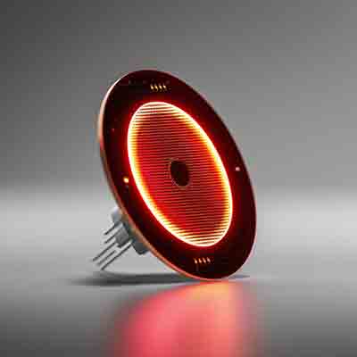
Can you get AlGaInAs LED wafers with emission wavelength around 650 nm?
AlGaInAs LED Wafers
A PhD professor at a Nanophotonics Center requested a quote for the following.
Pls see below for the offer on required epi wafer
AlGaInAs LED Wafer Red Color
Wafer Size : 4’’
Substrate : Planar Single side polished GaAs
Substrate thickness & Flat type 4’’ 350 um,Semi flat
Dominant Wavelength : 650nm
Reference #147024 for specs and pricing.
Get Your Silicon Wafer Quote FAST! Or, Buy Online and Start Researching Today!
How are Gallium Arsenide Wafers Used to Fabricate Light Emitting Diodes (LEDs)?
Gallium arsenide (GaAs) wafers are used in the fabrication of Light Emitting Diodes (LEDs) primarily in the following ways:
-
Substrate Material: GaAs wafers serve as the substrate on which the LED
 layers are deposited. The crystalline structure and properties of GaAs provide a stable foundation for growing epitaxial layers of semiconductor materials.
 -
Epitaxial Growth: Layers of different semiconductor materials, such as gallium nitride (GaN) for blue or green LEDs, are grown on the GaAs substrate using techniques like molecular beam epitaxy (MBE) or metalorganic chemical vapor deposition (MOCVD). These layers include the active region where electron-hole recombination occurs to emit light.
-
Electrical Contacts: GaAs wafers can be used to form the electrical contacts and connections needed for the LEDs. Metal contacts are typically deposited on the GaAs substrate to facilitate electrical current injection into the LED structure.
-
Performance Benefits: LEDs fabricated on GaAs wafers can offer advantages such as high efficiency, fast response times, and the ability to emit light at various wavelengths across the spectrum, depending on the specific semiconductor materials used in the epitaxial layers.
In summary, GaAs wafers provide a stable and efficient platform for growing the semiconductor layers necessary for manufacturing high-performance LEDs with different colors and properties.
