We need SiO2/Si wafer with 300nm of sio2 layer for optical microscope characterization of graphene. If square wafer of size< 2.5cm x 2.5cm is available is preferred with thickness of 5mm or above. please reply as soon as possible.
Optical Microscope for Researchers
Optical Microscope Characterization
A PhD candidate requested a quote for the following.
Reference #99673 for specs and pricing.
Get your Undoped Silicon Quote FAST! Buy online and start researching today!
What Is An Optical Microscope and Why is it Necessary in Semiconductor Research?
An optical microscope is a device that uses visible light and lenses to magnify small objects, allowing observation of details not visible to the naked eye. It typically employs a combination of lenses (objective and eyepiece) to produce an enlarged image of a sample placed on a stage.
Why it's necessary in semiconductor research:
-
Inspection and Quality Control:
Optical microscopes help researchers visually inspect semiconductor wafers for surface defects, particles, contamination, cracks, scratches, and structural irregularities.
 -
Photolithography Process Verification:
In semiconductor manufacturing, optical microscopes verify alignment accuracy, mask pattern transfer fidelity, and the uniformity of photoresist coatings, crucial for high-quality device fabrication. -
Metrology (Measurement):
They are used to measure critical dimensions of semiconductor structures, including line widths, feature sizes, and layer thicknesses, ensuring designs meet precise specifications. -
Failure Analysis:
In research and production, optical microscopy is essential for diagnosing failure mechanisms such as shorts, opens, delamination, corrosion, and other physical anomalies. -
Rapid and Cost-effective Analysis:
Compared to advanced electron microscopy methods (like SEM or TEM), optical microscopy is simpler, faster, non-destructive, cost-effective, and can provide immediate visual feedback during production. -
Real-Time Process Monitoring:
Researchers use optical microscopy to monitor semiconductor fabrication processes (etching, deposition, doping, and polishing) in real-time, enabling adjustments that enhance process control.
In summary, optical microscopy remains a foundational tool in semiconductor research due to its simplicity, versatility, affordability, rapid analysis capability, and essential role in both development and quality assurance processes.
Which part of an optical microscope contains a magnifying lens?
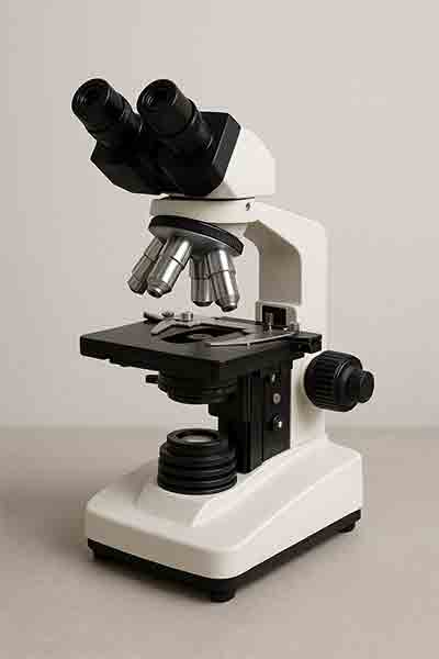
The objective lens and the eyepiece (ocular) lens are the two main parts of an optical microscope that contain magnifying lenses:
-
Objective Lens:
-
Located near the sample.
-
Provides the primary magnification.
-
Most microscopes have several objective lenses on a rotating nosepiece (e.g., 4x, 10x, 40x, 100x).
-
-
Eyepiece (Ocular Lens):
-
Located at the top of the microscope where you place your eyes.
-
Typically provides additional magnification (commonly 10x).
-
The total magnification is calculated by multiplying the magnification power of the eyepiece lens by that of the objective lens.
For example:
If the eyepiece is 10x and the objective lens is 40x → Total magnification = 400x.
