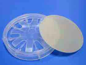
Sapphire Windows (Al2O3)
Sapphire Window Sale
Below are some of the Sapphire (Al2O3) that are on sale!

Get Your Quote FAST!
Buy Sapphire Windows Online and SAVE!
Compare our prices to competitors. We can beat any price!
Buy as few as one wafer, or buy in volume!
Below are just some of the sapphire windows that we have in stock.
Please let us know if you can use or provide us with your specs/qty.
We can manufacture Sapphire up to 200mm in diameter!
| Item# | Dia | Ori | Thick (um) | Polish |
| 3156 | Rectangle | <0001> | 500um | SSP |
| 3467 | 10mmX10mm | <0001> | 430um | DSP |
| 3409 | 6.0mm | <0001> | 100um | DSP |
| 1251 | 50.8mm | <0001> | 430um | DSP |
| 1306 | 50.8mm | <0001> | 430um | SSP |
| 2768 | 50.8mm | <0001> | 330um | DSP |
| 3407 | 50.8mm | <0001> | 100um | DSP |
| 1732 | 100mm | <0001> | 650um | SSP |
| 2562 | 100mm | <0001> | 650um | DSP |
- 50.8mm Sapphire Wafers 430um DSP
- 76.2mm Sapphire Wafers 350um SSP
- 100mm Sapphire Wafers 600um DSP
- 150mm Sapphire Wafers
- 200mm Sapphire Wafers 1mm SSP
Other diameters/dimensions also available
Sapphire Window Orientations
- R-axis (10-12)
- C-axis (0001)
- A-axis (11-20)
- M-axis (11-10)
A-Plane Sapphire Window Inventory
- Al2O3 - Sapphire Wafer 5x5x0.5 mm, A plane (11-20), DSP
- Al2O3 - Sapphire Wafer 5x5x0.5 mm, A plane (11-20), SSP
C-plane Sapphire Window Inventory
Diameter: 50.8±0.1mm
Orientation: C-Plane(0001)
M- axis 0.2±0.1 deg off, A- axis 0±0.1 deg off
Primary flat orientation :
A-plane(11-20) ±0.3deg
Primary flat length: 16.0±1mm
Thickness: 400±15um
Bow: ≤10um
TTV: ≤10um
Micro-roughness: Ra≤0.3nm
Front surface finish: Epi-polished
Back surface finish: Fine Ground
Packing: vacuum-sealed in 25 wafers Email us for low pricing
Diameter: 50.8±0.1mm
Orientation: C-Plane(0001)
M- axis 0.2±0.1 deg off, A- axis 0±0.1 deg off
Primary flat orientation :
A-plane(11-20) ±0.3deg
Primary flat length: 16.0±1mm
Thickness: 400±15um
Bow: ≤10um
TTV: ≤10um
Micro-roughness: Ra≤0.3nm
Front surface finish: Epi-polished
Back surface finish: Epi-polished
Packing: vacuum-sealed in 25 wafers Email us for low pricing
- Al2O3 Sapphire Wafer, C-plane (0001), 5x5x0.5mm, SSP
- Al2O3 Sapphire Wafer, C-plane (0001), 5x5x0.5mm, DSP
- Al2O3- Sapphire Wafer, C-plane (0001), 10mmx5mmx0.5mm, DSP
- Al2O3 - Sapphire Wafer, C-plane (0001), 10x10x0.1mm, DSP
- Al2O3- Sapphire Wafer, C-plane (0001), 10x10x0.1mm, SSP
Which keyword did you use to find us?
Let us know and we'll discount your order!
- Sapphire wafer
- Sapphire wafer cost
- Sapphire wafer manufacturers
- Sapphire wafers price
- Sapphire wafers rubicon
- Sapphire wafer properties
- Sapphire wafer polishing
- Sapphire wafer market
- Sapphire wafer led
- Sapphire wafer cleaning
- Sapphire wafer production
- Sapphire windows
- Optical sapphire
- Optical sapphire properties
- Optical sapphire transmission
- Optical sapphire window
- Optical sapphire glass
M-PlaneSapphire Window Inventory
- Al2O3 - Sapphire Wafer, M plane, 5x5x0.5mm, DSP
- Al2O3 - Sapphire Wafer, M plane, 5x5x0.5mm, SSP
R-Plane Sapphire Window Inventory
- Al2O3- Sapphire Wafe, R Plane, 5x5x0.5mm, SSP
