
What Are Silicon Wafer Grades?
Silicon wafer grades are categories used to describe wafers according to their intended application, surface condition, dimensional requirements, processing history, and overall quality level. Common terms include prime grade, test grade, monitor grade, mechanical grade, and reclaim silicon wafers.
These terms are useful when selecting silicon wafers for semiconductor fabrication, equipment testing, thin-film deposition, MEMS, process development, and materials research. However, wafer-grade terminology should not be interpreted as a universal specification standard. Exact requirements can vary by wafer manufacturer, supplier, diameter, process generation, and intended application.
Researchers should therefore evaluate the actual wafer specifications rather than selecting a substrate solely because it is described by a particular grade name.
Prime Grade Silicon Wafers
Prime grade silicon wafers are generally the highest-quality category intended for demanding semiconductor processing and research. Prime wafers typically have tightly controlled surface quality, wafer geometry, crystal properties, cleanliness, and electrical specifications appropriate for their intended fabrication process.
Prime-grade substrates are commonly selected when wafer quality can directly influence device fabrication or experimental results. Applications can include photolithography, oxidation, thin-film deposition, epitaxial growth, microfabrication, semiconductor devices, and surface-sensitive research.
Depending on the specification, a prime wafer may be supplied as single-side polished (SSP) or double-side polished (DSP). The required surface finish should be selected according to the fabrication process rather than assuming that every prime wafer has identical polishing requirements.
When Should You Use Prime Grade Wafers?
Prime silicon wafers are generally appropriate when the starting substrate must satisfy relatively demanding requirements for surface condition, geometry, cleanliness, or crystal quality. They are particularly useful when defects or dimensional variations could interfere with subsequent processing.
Typical research and fabrication uses can include:
- Semiconductor device fabrication
- Photolithography and pattern transfer
- Thin-film deposition
- Thermal oxidation
- MEMS and microfabrication
- Wafer bonding
- Surface and interface research
- Epitaxial growth when the wafer meets the required epi-ready specifications
For processes involving crystalline layer growth, an appropriately prepared surface may be required for silicon epitaxy . "Prime grade" alone should not automatically be assumed to mean that a wafer satisfies every epitaxial process requirement.
Test Grade Silicon Wafers
Test grade silicon wafers are commonly used for process development, equipment qualification, training, deposition experiments, etch testing, and other work where full prime-grade specifications may not be necessary.
Test wafers can provide a lower-cost substrate for developing a process before valuable device wafers are introduced. Depending on the supplier and lot, test-grade material may have relaxed specifications for parameters such as surface defects, geometry, cosmetic appearance, electrical properties, or other characteristics.
Because the meaning of test grade varies, researchers should confirm which parameters are guaranteed before using these wafers for an experiment that depends on a particular resistivity, orientation, thickness, surface condition, or geometry.
Monitor Silicon Wafers
Monitor wafers are used to evaluate and track semiconductor fabrication processes. Rather than becoming the final product, a monitor wafer can travel through selected processing steps so that engineers and researchers can measure the effect of the process.
Monitor wafers can be used during oxidation, deposition, etching, cleaning, implantation, diffusion, annealing, polishing, and other fabrication operations. Measurements performed on these wafers can help evaluate parameters such as film thickness, uniformity, sheet resistance, contamination, particles, surface condition, or process repeatability.
For example, a silicon monitor wafer can be processed alongside other wafers during thermal oxidation and subsequently measured to evaluate oxide thickness and uniformity.
Test Wafers vs. Monitor Wafers
The terms test wafer and monitor wafer can overlap in practical usage, but they describe different concepts. A test-grade designation generally refers to the wafer's quality category or intended economical use, while a monitor wafer describes the role that the wafer performs within a fabrication or process-control sequence.
A wafer used as a process monitor does not necessarily belong to one universal "monitor grade." Its required specifications depend on what is being measured. Some monitoring applications may tolerate inexpensive substrates, while others require highly controlled starting wafers so that small process changes can be measured reliably.
Mechanical Grade Silicon Wafers
Mechanical grade silicon wafers are generally selected for applications in which mechanical dimensions, handling characteristics, or basic substrate properties are more important than semiconductor-device-grade surface or electrical performance.
Depending on supplier specifications, these wafers can be useful for equipment setup, handling tests, fixtures, training, mechanical experiments, demonstrations, or preliminary process trials.
Mechanical-grade material should not automatically be assumed suitable for processes requiring tightly controlled surface roughness, defect density, resistivity, minority-carrier properties, or other semiconductor-grade characteristics unless those parameters are specifically provided.
Reclaim Silicon Wafers
Reclaim silicon wafers are previously processed silicon substrates that have undergone controlled processing intended to remove existing films, patterns, residues, or damaged surface material so that the wafer can be reused for appropriate applications.
The silicon wafer reclaiming process can involve operations such as film removal, cleaning, surface treatment, polishing, and inspection, depending on the condition of the incoming wafer and the specifications required for reuse.
Reclaim wafers can be economical for equipment monitoring, deposition and etching trials, process development, training, and other applications that do not require a new prime substrate.
Prime vs. Reclaim Silicon Wafers
The appropriate choice between prime and reclaim silicon wafers depends on the process. Prime wafers are generally preferred when tightly controlled starting material is important to device performance or experimental reproducibility.
Reclaim wafers can be appropriate when the substrate primarily serves as a process carrier, monitor, or development wafer and its specifications satisfy the experiment. Reclaim processing removes some silicon and can alter wafer thickness and geometry, so reclaimed substrates should be evaluated against the requirements of the intended equipment and process.
Research Grade Silicon Wafers
The term research grade silicon wafer is often used broadly for substrates intended for laboratory, university, prototype, or development work. It should not be interpreted as a universally standardized semiconductor grade.
Research applications vary widely. One experiment may require a highly polished prime wafer with tightly specified resistivity, while another may only require an inexpensive silicon substrate of known orientation and approximate thickness.
Researchers should therefore select wafers according to the parameters that actually affect the experiment instead of relying only on the phrase "research grade."
Wafer Grade vs. Wafer Specifications
A silicon wafer grade does not replace the detailed specifications needed to define a substrate. Two wafers described using the same general grade may still differ substantially in their electrical, crystallographic, dimensional, and surface properties.
Important specifications can include:
- Silicon crystal growth method, such as CZ or FZ
- Crystal orientation, such as (100), (111), or (110)
- P-type or n-type conductivity
- Dopant species
- Electrical resistivity
- Wafer diameter
- Wafer thickness
- Total thickness variation (TTV)
- Bow and warp
- Single-side or double-side polishing
- Surface roughness and defect requirements
- Edge configuration and other dimensional requirements
Researchers requiring specific electrical characteristics can also select p-type silicon , n-type substrates, high-resistivity material, or heavily doped silicon wafers according to the needs of the experiment.
Surface Quality and Silicon Wafer Grade
Surface quality can be especially important when selecting wafers for photolithography, thin-film deposition, oxidation, bonding, epitaxy, or nanoscale characterization. Scratches, particles, pits, haze, contamination, and surface roughness can interfere with some processes even when they are unimportant for others.
High-quality polished surfaces can be produced using processes that include chemical mechanical polishing (CMP) . Surface requirements should be matched to the experiment rather than assuming that every application requires the highest available wafer grade.
How to Choose a Silicon Wafer Grade
Choosing the correct silicon wafer grade begins by identifying which wafer properties actually affect the process. A semiconductor device experiment may require prime-quality material, while deposition calibration or equipment testing may be performed successfully with test, monitor, or reclaim wafers that meet the necessary specifications.
Before ordering, consider the required orientation, conductivity type, resistivity, thickness, diameter, surface finish, wafer geometry, processing history, and acceptable defect level. This approach can provide a better balance between experimental requirements and substrate cost.
UniversityWafer supplies silicon wafers for semiconductor fabrication, process development, equipment testing, MEMS, thin-film deposition, microfabrication, university laboratories, and materials research.
Get Your Silicon Wafer Quote FAST!
Or,
Buy Wafers Online
and Start Researching Today!
Choosing a Silicon Wafer Grade by Application
Selecting the correct silicon wafer grade depends on which substrate properties are critical to the experiment or fabrication process. The highest available grade is not automatically necessary for every application. In many cases, test, monitor, mechanical, or reclaim wafers can provide a more economical substrate when their specifications satisfy the requirements of the process.
Researchers should evaluate the actual silicon wafer specifications rather than relying only on labels such as "prime" or "test." Important parameters can include crystal orientation, conductivity type, dopant, resistivity, thickness, surface finish, wafer geometry, defect requirements, and processing history.
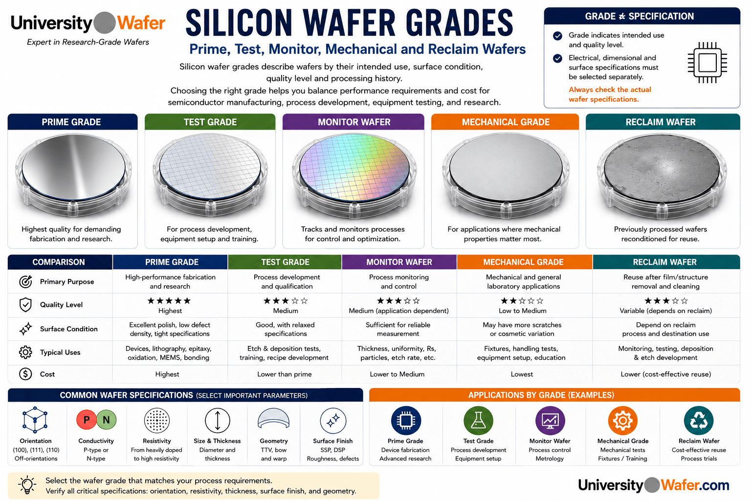
Silicon Wafer Grade Comparison
The following comparison provides a general guide to common semiconductor wafer grades. Exact definitions and acceptance criteria can vary among manufacturers and suppliers, so the individual wafer specification should always be checked before use.
| Wafer Category | Typical Purpose | Common Applications |
|---|---|---|
| Prime Grade | Demanding fabrication and research requiring controlled substrate quality | Devices, lithography, oxidation, deposition, MEMS, surface research |
| Test Grade | Process development and equipment testing | Etch tests, deposition trials, training, process setup |
| Monitor Wafer | Tracking or characterizing a fabrication process | Film thickness, uniformity, particles, sheet resistance, process control |
| Mechanical Grade | Applications emphasizing physical substrate properties rather than device-quality electrical performance | Handling tests, fixtures, equipment setup, mechanical experiments |
| Reclaim Wafer | Reuse after removal of previous films or structures and appropriate surface reprocessing | Monitoring, equipment qualification, deposition and etch development |
Prime Grade Wafers for Semiconductor Fabrication
Prime grade silicon wafers are generally selected when starting-substrate quality can significantly influence fabrication yield, device behavior, or experimental reproducibility. Semiconductor processing may involve photolithography, oxidation, implantation, diffusion, deposition, etching, annealing, and metallization, all of which can place different requirements on the starting wafer.
Prime material is particularly useful for semiconductor device manufacturing when controlled wafer geometry, surface quality, cleanliness, electrical properties, and crystallographic characteristics are required.
Test Wafers for Process Development
Test silicon wafers can be useful when developing a new fabrication process before running more valuable device wafers. Engineers may use test wafers to establish equipment conditions, determine etch rates, evaluate deposition recipes, develop lithography processes, or study thermal treatments.
For example, a test wafer can be used to determine whether a deposition process produces the desired thickness and uniformity before the same recipe is applied to higher-value substrates.
Test-grade material should still meet all specifications relevant to the experiment. A lower grade is only useful when its relaxed characteristics do not interfere with the measurement being performed.
Monitor Wafers for Process Control
Silicon monitor wafers provide a convenient substrate for measuring the performance and stability of semiconductor fabrication equipment. They can be processed periodically or alongside production and experimental wafers to evaluate process behavior.
Depending on the process, monitor wafers can be used to measure:
- Deposited film thickness and uniformity
- Thermal oxide thickness
- Sheet resistance
- Etch rate and etch uniformity
- Particle contamination
- Surface condition
- Process repeatability
A monitor wafer should have sufficiently controlled starting properties for the measurement of interest. Otherwise, variation in the substrate itself can make it more difficult to distinguish actual process variation.
Silicon Wafers for Thin-Film Deposition
Silicon is widely used as a substrate for thin-film deposition because polished wafers provide smooth, stable surfaces compatible with many vacuum and chemical processing techniques.
Prime wafers may be appropriate for demanding interface or device studies, while test and reclaim wafers can often be useful for deposition calibration, film-thickness measurements, stress experiments, and preliminary process development.
When depositing silicon dioxide, researchers may also compare deposited films with thermally grown silicon dioxide , which is formed by consuming silicon at the substrate surface rather than depositing material onto it.
Silicon Wafer Grades for Photolithography
Photolithography can place demanding requirements on wafer surface quality and geometry. Surface particles, scratches, contamination, bow, warp, and thickness variation can affect resist coating, exposure, focus, alignment, and pattern transfer.
Prime wafers are therefore commonly selected for demanding lithography and device fabrication. Test wafers can still be valuable for photoresist coating trials, exposure optimization, equipment setup, and training when their surface and geometric properties are adequate for the process.
Silicon Wafer Grades for Etching
Test and monitor wafers are frequently useful for developing silicon and thin-film etching processes. They can be used to evaluate etch rate, selectivity, uniformity, surface condition, and process repeatability before more valuable substrates are processed.
When silicon itself is being etched, crystal orientation can become an important specification. In anisotropic silicon etching , certain wet etchants exhibit different etch rates for different crystallographic planes. The wafer orientation therefore directly influences the resulting structure.
Wafer Grades for MEMS Research
MEMS silicon wafers may require particularly careful selection because device fabrication can depend on both surface and bulk substrate properties. Crystal orientation, thickness, TTV, bow, resistivity, polishing, and backside condition can all be important.
Prime or tightly specified wafers are often appropriate for final MEMS structures, while lower-cost test wafers may be useful for developing lithography, etching, bonding, and deposition processes.
Double-side polished substrates can be particularly useful when processing, alignment, optical inspection, or patterning is required from both sides of the wafer.
Single-Side Polished vs. Double-Side Polished Wafers
Wafer grade and polishing configuration are separate specifications. A single-side polished (SSP) wafer has one major surface polished to the specified finish, while a double-side polished (DSP) wafer has both major surfaces polished.
SSP wafers are suitable for many semiconductor and thin-film processes in which only the front surface requires a high-quality finish. DSP wafers are useful for MEMS, wafer bonding, backside processing, optical applications, and experiments requiring access to both surfaces.
CZ vs. FZ Silicon Wafer Grades
Wafer grade should also be distinguished from the method used to grow the silicon crystal. Both Czochralski (CZ) and float-zone (FZ) silicon can be supplied with different quality and surface specifications.
Czochralski silicon is grown from a silicon melt contained in a crucible and is widely used throughout semiconductor manufacturing. Conventional CZ silicon generally contains more oxygen than FZ material because oxygen can enter the melt from the silica crucible.
Float-zone silicon is grown without a crucible contacting the molten zone and generally has lower oxygen content. FZ silicon is also commonly available at high resistivity, making it useful for detectors, RF structures, and other specialized applications.
Does Wafer Grade Determine Resistivity?
Wafer grade does not determine silicon resistivity. Resistivity is an electrical material specification related to carrier concentration and mobility, whereas grade generally describes quality, intended use, or acceptance criteria.
A prime wafer can be highly doped or high resistivity depending on its specification. Similarly, a test wafer may be supplied within a particular resistivity range if that property is required.
Researchers requiring low-resistivity substrates can consider heavily doped silicon wafers , while high-resistivity silicon can be selected for applications where substrate conduction must be reduced.
Does Wafer Grade Determine Crystal Orientation?
Crystal orientation is also independent of wafer grade. Silicon wafers can be cut with surface orientations such as (100), (111), or (110), depending on the application and material availability.
Orientation affects properties and processes including anisotropic etching, oxidation kinetics, surface atomic structure, cleavage behavior, and some epitaxial and device-processing requirements.
Researchers should therefore specify both the required wafer grade and crystal orientation.
Surface Roughness and Wafer Grade
Surface roughness is particularly important for processes involving nanoscale films, interfaces, wafer bonding, epitaxy, or surface characterization. However, a grade name alone does not provide a complete quantitative description of surface roughness.
Silicon surfaces can be finished using processes including chemical mechanical polishing (CMP) . When surface roughness is critical, the required roughness metric, measurement scale, and acceptance limit should be specified explicitly.
Understanding Reclaim Wafer Limitations
Reclaim silicon wafers can significantly reduce substrate costs for appropriate process-development and monitoring applications, but they should not automatically be treated as equivalent to new prime wafers.
Reclaim processing can remove some silicon from the substrate, potentially changing wafer thickness and other geometric characteristics. The previous processing history can also be relevant when contamination or other application-specific requirements are especially strict.
A properly specified reclaimed silicon wafer can nevertheless be highly useful for deposition, etching, cleaning, equipment qualification, and process-monitoring applications.
Wafer Geometry: TTV, Bow and Warp
Total thickness variation (TTV), bow, and warp describe different aspects of silicon wafer geometry. These parameters can influence lithography, bonding, chucking, polishing, handling, deposition, and other fabrication processes.
TTV describes the difference between the maximum and minimum wafer thickness over a specified measurement region. Bow and warp characterize wafer shape using different reference definitions and should not be treated as interchangeable measurements.
Applications requiring tight dimensional control should specify acceptable geometry limits instead of relying solely on a wafer-grade designation.
How to Specify Silicon Wafers for Research
When ordering research silicon wafers, provide the specifications that matter to the experiment. A useful wafer request can include:
- Wafer grade or intended application
- Diameter
- Thickness
- Crystal orientation
- Growth method: CZ or FZ when important
- P-type or n-type conductivity
- Dopant species
- Resistivity range
- SSP or DSP surface finish
- TTV, bow, or warp limits when required
- Surface roughness or defect requirements when critical
- Quantity
Providing these parameters makes it easier to identify a silicon wafer that matches the actual research or fabrication requirements instead of choosing solely by a general grade label.
Which Silicon Wafer Grade Should You Choose?
For demanding device fabrication or surface-sensitive experiments, prime grade silicon is generally the appropriate starting point. For equipment setup and process development, test grade wafers can provide a more economical option. Monitor wafers are selected according to the process parameter being tracked, while reclaim wafers can be valuable when reuse is compatible with the application's contamination, thickness, geometry, and surface requirements.
The key is to match the substrate specification to the process. UniversityWafer supplies silicon substrates for semiconductor fabrication, MEMS, microfabrication, thin-film deposition, process development, equipment qualification, and university research.
Related Silicon Wafer Resources
- Silicon Wafers – Explore silicon substrates by diameter, crystal orientation, conductivity type, resistivity, thickness, and surface finish.
- Bulk Silicon Wafers – Learn about bulk single-crystal silicon, including CZ and float-zone substrates, doping, resistivity, orientation, and wafer specifications.
- Czochralski Silicon Wafers – Learn how the Czochralski process is used to grow single-crystal silicon ingots for semiconductor wafer production.
- Silicon Wafer Reclaiming – Explore wafer reclaim processes used to prepare previously processed silicon substrates for appropriate reuse and process-development applications.
- Chemical Mechanical Polishing (CMP) – Learn how CMP is used to produce smooth, controlled silicon surfaces for semiconductor processing and research.
- P-Type Silicon Wafers – Learn about acceptor-doped silicon and how doping influences carrier concentration, conductivity, and wafer resistivity.
- Heavily Doped Silicon Wafers – Explore low-resistivity silicon substrates for semiconductor, electrochemical, MEMS, and materials research.
- Silicon Doping and Carrier Mobility – Learn how dopant concentration affects carrier concentration, mobility, conductivity, and silicon resistivity.
- Silicon Epitaxial Wafers – Explore epitaxial silicon layers and substrate requirements for semiconductor device fabrication and research.
- Silicon-on-Insulator (SOI) Wafers – Compare conventional silicon substrates with engineered SOI wafers containing a device layer and buried insulating layer.
- Thermal Oxide on Silicon Wafers – Learn about thermally grown SiO2 for dielectric layers, masking, MOS structures, MEMS, and semiconductor processing.
- Silicon Wafers for Anisotropic Etching – Explore how silicon crystal orientation affects anisotropic wet etching and MEMS microfabrication.
- Semiconductor Device Manufacturing – Learn how silicon wafers are processed through oxidation, lithography, etching, doping, deposition, annealing, and metallization.