Silicide On Insulator (SSOI) Substrates
Get Your Quote FAST!
What is Silicon On Silicide On Insulator (SSOI) Substrates?
Silicon on silicide on insulator (SSOI) substrates are a type of microelectronic substrate that consists of a layer of silicon on top of a layer of silicide on top of an insulating layer. The insulating layer is typically made of silicon dioxide (SiO2) and is used to isolate the silicon and silicide layers from the substrate below, which is typically made of bulk silicon.
One advantage of SSOI substrates is that the silicide layer can help to reduce the resistance of the silicon layer, which can lead to faster switching speeds and lower power consumption. The insulating layer also helps to reduce parasitic capacitance, which can further improve device performance.
In addition, SSOI substrates can allow for the creation of devices with very thin layers of silicon, which can be useful for some applications. They are also compatible with a variety of semiconductor manufacturing processes, making them a versatile choice for microelectronic device fabrication.
Why Use Silicon on Silicide on Insulator Wafers?
If you're in the market for a new type of insulator substrate, you might want to learn what 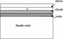 Silicon on Silicide is. It's an extremely effective insulator that offers excellent conductivity and moisture resistance. This material is a great choice for use in electrical and electronic circuits, and is often used in the manufacturing of semiconductors. However, its use is limited, and not all manufacturers have it on their insulator substrates.
Erbium silicide
Erbium silicide on insulation substrates is one of the hottest topics in semiconductor technology. This is because the rare earth metal typified by erbium (Er) has a high Schottky barrier to electrons. Therefore, erbium silicide can be a useful material for a plethora of CMOS and PMOS devices. The encapsulation process for erbium silicide on insulation substrates should be done with caution because of the low-temperature oxidation resistance of the metal substrates.
One way to achieve this is through the use of a hybrid coating system. This is usually made up of a silicon nitride film and a silicon oxide film. As a result, the encapsulation process can be made faster and easier. The result is a high temperature resistant coating with its own advantages.
The aforementioned high-temperature resistant coating process deserves a more in-depth study. A typical semiconductor device comprises a semiconductor substrate, a source-drain diffusion layer, a metal source/drain layer, a nickel silicide layer, a polysilicon film, a side wall, a hard mask material, and a first gate insulation film. In this instance, the aforementioned insulating particles have been arranged in the first gate electrode 61. Likewise, the second gate electrode 12 carries out the aforementioned functions on the second gate insulation film 52.
The most efficient encapsulation process is the one where the aforementioned layers are combined. An upper portion of the first gate insulation film is a silicon nitride film, while the lower portion is a silicon oxide film. As aforementioned, a second gate insulation film is also formed on the second gate electrode 12. Hence, a hybrid coating process is a necessity to produce a functional CMOS device.
Vanadium silicide
Vanadium silicide is an intermixing layer of Si and V formed by silicidation of metallic vanadium layers on silicon-on-insulator substrates. It is typically a type II superconductor. However, its critical temperature is the highest known.
Typical method to synthesize bulk V3Si involves melting the metals at a high temperature in an inert atmosphere. Nevertheless, a new approach to synthesis has recently been developed. This technique is suitable for CMOS fabrication. The thin films of V3Si have been previously prepared by electron-beam co-evaporation of V and Si.
A further step is annealing the film. Annealing enables the buildup of strain. If the strain is too large, the final silicide film may be porous. To avoid such a situation, the stoichiometry of the target must be precise. In addition, the interface must be controlled in terms of impurities.
X-ray photoeletron spectroscopy (XPS) is used to verify the composition of the vanadium silicide. XPS data indicates that the film is comprised of a 3:1 V:Si ratio. Also, the oxidative state of V3+ corresponds to 513 eV. XPS shows that the surface of the sample has a fine grain size.
EDX mapping images were also collected. These are collected simultaneously over the same area using the FEI Talos F200X microscope. They show that the top layer is a pure V layer, while the bottom layer is a mixed layer. EDX analysis shows that the Si2p peak position is near the elemental Si.
X-ray diffraction spectra of V films on SOI were measured before annealing and after vacuum annealing. Measurements of the diffraction spectra of the V films showed that they were in the A15 phase.
Nickel silicide
Nickel silicides are semiconductor nanostructures formed by the chemical reaction of Ni and Ti under an H2 atmosphere. These materials are characterized by a layered structure and the presence of a Ni3Si phase. Depending on the atomic concentration of these two metals, the nanomaterials vary in shape, thickness and polydispersity.
The chemical composition of the silicides is influenced by the concentration ratio of SiHCl3 and H2 used in the synthesis process. For example, the higher the concentration of SiHCl3 to H2, the greater the proportion of Ni3Si. The stoichiometric formation of the nanomaterials is facilitated by the low temperature synthesis and the atmospheric pressure method.
Several aspects of the invention include methods of forming conductive lines with nickel silicides on insulation substrates. One such method involves the use of a negative bias potential at -1.5 V to image defects related to the formation of nickel silicides.
Other aspects of the invention involve a colloidal approach to obtaining a controlled solvation and nucleation for nickel silicides. This allows the nanostructures to be formed at temperatures lower than the annealing of nickel silicides. It can also provide a high degree of phase purity and a low polydispersity.
For example, a Ni/Ti(1 nm)/Si system has been prepared by a one-step RTA. A titanium layer 42 has been deposited over the nickel 40. Both layers are then etched to remove the unreacted nickel.
In another embodiment, the substrate is a monocrystalline silicon wafer. However, the substrate could be an assembly of other materials, such as silicon nitride, undoped silicon dioxide, elemental nickel, cobalt, or other nickel-containing material.
A preferred substrate is a monocrystalline silicon substrate. An alternative substrate is a semiconductor-on-insulator substrate.
SiO2 with boron and phosphorus to improve moisture resistance and reflow characteristics
Phosphorus and boron have been used for many years as additives to silicon dioxide (SiO2) to enhance moisture resistance and reflow characteristics on insulator substrates. They do not need to be incorporated into the glass or a crystalline structure, but can fit through pores in the oxide lattice.
A phosphorus and boron modified silicon dioxide has a relatively low diffusion length compared to pure SiO2, and a significant improvement in the time to breakdown. However, the true solid-state diffusivity is not very impressive.
In the real world, most research on boron and phosphorus diffusion in oxides has centered on the process at high temperatures. Nevertheless, researchers have not found a reliable method to measure boron and phosphorus diffusion in the sub-ambients of typical flow processes.
The first and most obvious way to measure diffusion through thick oxides is by looking at changes in the flatband voltage of the MOS capacitors on the oxide. This can be done using a variety of techniques.
Another interesting and simple measurement is to look at how fast the liquid/solid mixture dissolves. This can be quantified using neutron activation analysis. Obviously, it is inconvenient to do this directly, but the results are in principle quantitative.
Most boron and phosphorus diffusion data are dated. Most of the data was gathered in the '70s or earlier. Moreover, the magnitude of the most significant boron and phosphorus diffusion is not very large.
Boron and phosphorus in the sub-ambients of typical flows penetrates less than 100 A into an undoped SiO2 film. Typical flow temperatures do not liquify enough to permit a rapid dissolution.
While it has not been proven to be a magic bullet for reflow properties, a higher fluorine concentration can reduce boron and phosphorus diffusion. It can also reduce the number of bonds between the silicon atoms.
Silicon-on-Sapphire
Silicon-on-sapphire is a type of semiconductor technology used in microelectronic circuits. This type of technology has several advantages including better isolation, low parasitic capacitance, and low power consumption. It has also gained increased traction in higher volume applications.
The Silicon-on-sapphire substrate provides a good combination of physical properties, such as thermal stability and electrical breakdown field. Therefore, this material is ideal for a wide range of electronic substrates.
Aside from being a good insulator, sapphire has excellent corrosion resistance. Moreover, its high thermal conductivity helps to balance generated heat. In addition, it is very hard, strong, and durable. Thus, it can be used in high pressure environments.
Currently, sapphire is the main material for silicon epitaxial substrates. However, there are other materials which are better. For instance, spinel substrates are a much better option for large-scale integrated circuits. They are more insulating, have good lattice matching, and can be fabricated by epitaxial growth of silicon.
These benefits make the use of a spinel substrate an attractive option for high-power radio frequency applications, such as satellite communication systems. Additionally, it can increase radiation resistance and eliminate the need for multiple component connections in integrated circuits.
Silicon-on-sapphire (SOS) technology was developed in the 1970s by the California Institute of Technology. It has since been commercialized. But, there have been many challenges for the technology, particularly in a commercial sense.
One major challenge faced by the SOS technology is the development of small transistors. Furthermore, the process of manufacturing is also expensive. Nevertheless, the substrate provides a superior substrate for various electronic applications, enabling better integration of analog and digital circuitry. Besides, it is also resistant to wear and mechanical damage, which means it is durable and can withstand harsh conditions.