Aluminum Nitride on Sapphire Wafers for Research& Production
Recent AlN on Sapphire Wafer Sales
A researcher requested the following:
UniversityWafer, Inc. quoted the following:
Single-crystal Aluminum Nitride (AlN) onto Silicon <111> substrates. 6-inch wafers,thickness of the AlN wafer is 1400 nm. Furthermore, 500 nm PECVD SiO2 capping layer on top
Single-crystal Aluminum Nitride (AlN) onto Sapphire <0001> substrates. 6-inch wafers,thickness of the AlN wafer is 1400 nm. Furthermore, 500 nm PECVD SiO2 capping layer on top.
Get Your AlN Wafer Quote FAST!
GaN, AlN Templates to Grow 2D Tranistion Metal Dichalcogenides.
A researcher requested we help them with their research.
I am interested in GaN templates, AlN templates (if available), and hBN (if available).The goal is to grow 2D transition metal dichalcogenides and measure their electrical properties, so these templates need to be highly insulating with negligible electrical mobilities, so as no to contribute any spurious electrical signal to the 2D materials on top.
For semi insulating GaN templates, the typical specifications are as follows. Size = 2", Single crystal/highly epitaxial grown on cAl2O3, single side polished, resistivity > or ~ 10^6 ohm cm. Quantity = 1-2 pieces. (based on price per piece). Please tell me if Gallium polar or Nitrogen polar can be obtained.
For semi insulating AlN templates, the typical specifications are as follows. Size = 2", Single crystal/highly epitaxial grown on cAl2O3, single side polished. resistivity > 1 x 10^6 ohm cm. Quantity = 1-2 pieces. (based on price per piece). Please tell me if Aluminium polar or Nitrogen polar can be obtained.
For hBN, the typical specifications are as follows. Size = 10 mm x 10 mm pieces on SiO2/Si. Resistivity > 1 x 10^6 ohm cm. Quantity = 5-10 pieces (based on price per piece).
I am currently growing some 2D transition metal dichalcogenides (2d TMDC) based semiconductors on III Nitride templates such as GaN and AlN. My goal is to study if there is some clear epitaxial growth between these two different materials. While we have got some promising results for growth on GaN, we are still studying what happens when we try to grow on AlN. So that's why there is some delay on placing the orders. Once we have established that the 2D materials can be grown on onto these semiconductors, then i will go forward with the orders. I also see that u have graphene on SiO2/Si that also another substrate that i am keen on exploring with regards to 2D TMDC.
Can u please send me a quote for 2",4"wafer of AlN/Si? And also similar quotes for GaN/Si
UniversityWafer, Inc. Quoted the Following:
2" wafer of AlN/Si, Size = 2", Single crystal/highly epitaxial AlN grown on Silicon, single side polished. resistivity > 1 x 10^6 ohm cm. Quantity = 1 pieces. Aluminium polar,AlN layer 25nm
Please contact us for pricing. Reference #253427
Aluminum Nitride on Sapphire
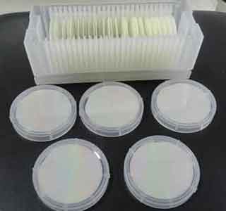
UniversityWafer Inc of South Boston, MA, USA, along with its partners, has introduced a new line of 50.8mm, 100mm and 150mm UV-grade aluminium nitride (AlN) on c-plane single-side-polished (SSP) sapphire and AlN-on-silicon prime-grade for high-electron-mobility transistor (HEMT) templates.

A major use of AlN-on-sapphire are ultraviolet (UV) LEDs. Some of the most powerful applications include irradiating hospital rooms and foundry cleanrooms, since AlN-on-sapphire LEDs disinfect instruments and can purify air and water of germs and bacteria without using chemicals.
The electricity savings of using LEDs instead of traditional cold-cathode fluorescent lamps (CCFLs) can reach 70%. Also, unlike CCFLs, AlN LEDs do not contain mercury, allowing more environmentally friendly disposal. AlN LEDs can also be used for non-line-of-sight communications.
Currently, the newest-generation AlN-on-sapphire LEDs technology is approaching 50,000 hours of life, compared with just 10,000 hours for existing AlN-on-sapphire LEDs. The cost saving will only increase with time, adds the firm.
UniversityWafer says that it carries a large inventory of AlN-on-sapphire substrates, and can also quote unique client specs in small quantities that make it feasible for budget-strapped researchers to obtain the substrates at a reasonable cost. Delivery time is also short, notes the firm. UniversityWafer hence caters to researchers who want both small quantities and short lead-times, with staff trained to handle even the most difficult low-volume requests.
For production, AlN-on-sapphire can be ramped up to meet a client’s demands in a timely and affordable manner, UniversityWafer adds.
Aluminum Nitride on Silicon
We also have a large selection of AlN on Silicon wafers. Recently a customer inquired:
UniversityWafer quoted:
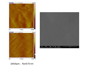
Dia. 6‘’ 200nm thick AlN on Silicon wafer Surface roughness: <1nm
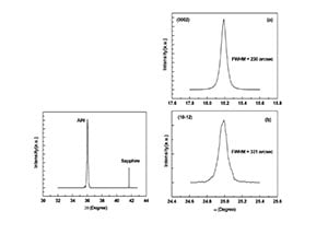
AlN Wafer Surface Roughness and XRD Linewidth
Researcher:
Can I get a quote for: AlN on Sapphire, c-axis orientated 6'' (001) Std SSP 200nm Un-doped,SI-type Prime Quantity: 2, or minimum order quantity Would also consider quantity 10 of 2" substrates.
UniversityWafer:
See below for the item more suitable for training purposes
2-2. AlN on Sapphire, c-axis orientated 2'' (001) Std SSP 100nm Un-doped,SI-type Prime Quantity: 10


What is Aluminum Nitride?
If you've ever wondered what is aluminum nitride, you've probably wondered what its potential applications might be. The material is a solid nitride of aluminium and has a very high thermal conductivity of up to 321 W. It also has excellent electrical insulator properties and has a band gap of about six eV at room temperature, making it a great material for optoelectronics.
 Besides its good thermal conductivity, Aluminum Nitride is also a good electrical insulator. It can be used in a wide variety of applications requiring superior electrical insulation. It is also known for its ability to resist corrosion. While most of the common uses of Aluminum nitride are in the electronics industry, it is increasingly found in the microelectronics field. In microelectronics, it is particularly useful due to its high thermal conductivity, which is unusual for an electrical insulator.
Aluminum nitride was first synthesized in 1877 and has many applications in microelectronics. It is a very good electrical insulator and has high thermal conductivity. Single crystals of the material have an extremely high thermal conductivity, making them ideal for a variety of electronic applications. In addition, it is stable in hydrogen atmospheres and has high thermal conductivity.
The material is stable at high temperatures under an inert atmosphere. It has a protective oxide layer that protects the material at up to 1370degC. It is also stable in hydrogen atmospheres up to 980degC. It can be dissolved or hydrolyzed by strong alkali, but is resistant to most molten salts and cryolite. This is why it is so useful in microelectronics.
The material is a good electrical insulator with excellent thermal conductivity. Its high insulating properties make it an excellent choice for a variety of applications. A wide variety of products can be made from aluminum nitride. This is the most common use for aluminum nitride. It is an important material in the aerospace industry. However, there are some limitations associated with it. It is unstable at high temperatures and in some environments.
A thin film of aluminum nitride is a layer of aluminum that is resistant to high temperatures. During high temperatures, this layer of aluminum will help protect the material. In high-pressure environments, it can be unstable. It can withstand a range of temperatures up to 980degC. At lower levels, it can be toxic to humans. It is also used in mobile phones. Its properties are extremely diverse.
Aluminum nitride is an electrically insulating material with low thermal conductivity. It is a versatile material that can be used in electronic devices and semiconductors. It has a very low coefficient of thermal expansion, which makes it a great material for a variety of applications. This compound is also a reliable and safe material for a semiconductor device. And because it has a low-toxicity, it is a good choice for a wide range of applications.
This material is highly conductive and has excellent electrical insulation. It is used in mobile phones for RF filters. The metal is also used for RF antennas. A thin film bar acoustic resonator made from AlN can detect radio signals. Its piezoelectric layer is also used for radar sensors. In addition to being an electrical conductor, it can be used in lasers, infrared detectors, and in lasers.
While aluminum nitride is an excellent electrical insulating material, it can be harmful to the body if it is exposed to it. It is used for solar cells and in a number of applications. But it is also a good material for microelectronics. Its melting point is around 2000 degrees Celsius, which makes it ideal for electronics. It also has an exceptional thermal conductivity for an electrical insulating material.
Aluminum nitride is a very interesting material with interesting properties. It is a semiconductor with a high boiling point, and has an extremely high thermal conductivity. It is also extremely resistant to electro-magnetic fields and electromagnets. Its properties make it an ideal material for electronics, but what is its purpose? It is used in a number of products, including computers and other electronic equipment.
