Researching Intense Radiation Effects on Materials with Different Band Gaps
A nuclear engineering graduate student requested semiconductor materials for research on
radiation-induced surface defects and the effects of intense radiation on materials with
different electronic band gaps.
Customer request, edited for clarity: I am researching the effects of
intense radiation on materials with different ionization energies. So far, I have primarily
studied gases, but I would now like to study
semiconductor materials
with different band gaps.
Because the samples will be exposed to intense radiation and may be damaged during testing,
I am interested in lower-cost pieces such as
diced wafers
,
broken wafers, or other suitable research-grade pieces. Samples approximately 1 cm or larger
in length and width would be useful. Thickness is not critical because the initial research
will focus on surface defects.
It would be ideal to obtain a variety of semiconductor materials, including
Si,
Ge,
GaAs,
InSb,
and
InAs,
with a combination of undoped, n-type, and p-type samples where available.
Reference #213033 for specs and pricing.
Get Your Semiconductor Material Quote FAST!
Or,
Buy Wafers Online
and Start Researching Today!
What Is a Semiconductor Band Gap?
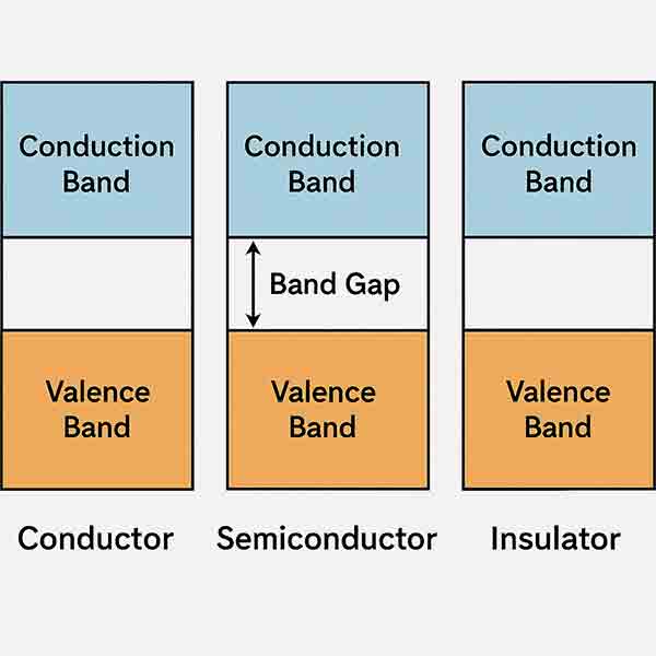
The band gap (Eg) is the energy difference between the
valence-band maximum and the conduction-band minimum of a material. It represents the
minimum energy required for an electron to be excited from the valence band into the
conduction band, where it can contribute to electrical conduction.
Band-gap energy is normally expressed in electron volts (eV). In general,
materials with very large band gaps have very low intrinsic carrier concentrations and
behave as electrical insulators, while semiconductors have band gaps that allow their
electrical properties to be controlled through doping, temperature, illumination, and
applied electric fields.
A smaller semiconductor band gap generally produces a higher
intrinsic carrier concentration at a given temperature because less
thermal energy is required to excite electrons across the gap. However, the actual
conductivity of a semiconductor also depends strongly on doping concentration, carrier
mobility, temperature, defects, impurities, and material quality.
The table below lists representative room-temperature band-gap values for several common
semiconductor materials, along with wide-gap silica materials for comparison. Exact values
can vary with temperature, crystal structure, composition, strain, and other material
conditions.
How Do You Determine the Energy Band Gap of a Material?
For crystalline solids, the electronic band gap is defined as the energy difference
between the valence-band maximum (VBM) and the
conduction-band minimum (CBM). The molecular terms HOMO and LUMO are more
commonly used for discrete molecules and molecular systems and should not generally be used
as direct substitutes for the valence and conduction bands of a bulk crystalline
semiconductor.
Band gaps can be determined experimentally or estimated through electronic-structure
calculations. The appropriate technique depends on the material, whether the transition
is direct or indirect, the sample geometry, and the accuracy required.
-
Experimental Methods
-
Optical Absorption Spectroscopy:
A semiconductor absorbs photons capable of producing electronic transitions.
Analysis of the absorption edge can be used to estimate the optical band gap.
The analysis must account for whether the material has a direct or indirect
transition and for effects such as disorder, excitons, defects, and sample thickness.
-
Photoluminescence Spectroscopy:
The material is optically excited and the emitted photons are analyzed.
Photoluminescence can provide valuable information about band-edge transitions,
excitons, impurities, and defects. The strongest emission peak does not necessarily
equal the fundamental band-gap energy in every material.
-
Photoconductivity:
Changes in electrical conductivity are measured while the sample is illuminated
with photons of different energies. The onset of photoconductivity can provide
information about electronic excitation thresholds and the band gap.
-
Electron Energy-Loss Spectroscopy (EELS):
EELS measures the energy lost by electrons as they interact with a thin specimen.
Low-loss EELS can provide information about electronic excitations and, with
appropriate analysis, can be used to investigate a material's band-gap region.
-
Computational Methods
Electronic-structure calculations can also be used to estimate semiconductor band
structures and band gaps. Density functional theory (DFT) is widely
used to calculate electronic structure, but common semilocal DFT approximations often
underestimate semiconductor band gaps.
More advanced approaches, including hybrid functionals and the
GW approximation, can provide improved predictions in many materials,
although they generally require greater computational resources and expertise.
Calculated values depend on the theoretical method, structural model, and material
conditions used in the calculation.
Because each technique measures somewhat different aspects of a material's electronic or
optical response, researchers may use several complementary methods when accurate band-gap
characterization is required.
FAQs About Band Gaps in Semiconductors
-
What is a band gap in a semiconductor?
-
The band gap is the energy difference between the valence-band maximum and the
conduction-band minimum. It determines the minimum energy required for band-to-band
electronic excitation and strongly influences a material's electrical and optical
properties.
-
Which materials are wide-bandgap semiconductors?
-
Important wide-bandgap semiconductors include
silicon carbide (SiC)
and gallium nitride (GaN). Their relatively large band gaps, together with properties
such as high critical electric fields, make them useful for many high-power,
high-voltage, high-temperature, and high-frequency applications. Fused silica and
quartz also have large electronic band gaps, but they are normally classified as
electrical insulators rather than wide-bandgap semiconductors.
-
Why is band gap important in
solar cells?
-
The semiconductor band gap influences which photon energies can generate electron-hole
pairs and affects the balance between solar-cell current and voltage. A smaller band gap
allows absorption of lower-energy, longer-wavelength photons and can increase potential
photocurrent, but it generally lowers the maximum attainable voltage. A larger band gap
can support a higher voltage but leaves more low-energy photons unabsorbed. Therefore,
photovoltaic design involves optimizing the band gap rather than simply choosing the
smallest possible value.
-
Does a smaller band gap make a semiconductor more conductive?
-
For an intrinsic semiconductor at a given temperature, a smaller band
gap generally produces a higher intrinsic carrier concentration and therefore higher
intrinsic electrical conductivity. In real semiconductor wafers, however, conductivity
also depends strongly on dopant concentration, carrier mobility, temperature, defects,
impurities, and material quality.
Low-Bandgap Semiconductors for Solar Cells and Photovoltaic Research
A graduate research assistant requested help with the following:
Can you please let me know if you have a low-bandgap semiconductor
that can be used to fabricate a solar or
photovoltaic cell
?
We would also like to know whether the doping profile of the material can be customized.
I can provide a research paper that we would like to follow to fabricate an
InAs
photodiode.
The doping profile discussed in the paper is described below.
The InAs wafer studied in the referenced work was grown by
metalorganic vapor-phase epitaxy (MOVPE) on a 2-inch p-type InAs
substrate. The epitaxial structure consisted of a 2 µm p+ InAs layer doped with Zn
at a nominal concentration of approximately 1 × 1018 cm−3,
followed by an 8 µm nominally intrinsic InAs layer and a 2 µm n+ InAs layer
doped with Si at approximately 1 × 1018 cm−3.
Band Gaps of Common Low-Bandgap Semiconductors
Representative room-temperature band-gap values for several common semiconductor materials
are listed below. Exact values can vary with temperature, crystal quality, composition, strain,
and other material conditions.
- Silicon (Si): approximately 1.12 eV
- Germanium (Ge): approximately 0.66 eV
- Indium Arsenide (InAs): approximately 0.35 eV
- Indium Antimonide (InSb): approximately 0.17 eV
Based on these values, low-bandgap materials such as
InAs
and
InSb
are especially useful for infrared optoelectronics, photodetectors, and other applications
requiring sensitivity to lower-energy, longer-wavelength photons.
Depending on current inventory and specifications, these materials may be available in
different diameters, conductivity types, doping levels, and crystallographic orientations.
Availability should be confirmed for the required wafer diameter, orientation, carrier
concentration, thickness, surface finish, and doping type.
We can also produce epitaxial structures using
MOCVD
or related epitaxial-growth techniques. Epitaxial structures can be designed with specified
layer thicknesses, compositions, and doping profiles, subject to material-system and growth-process
limitations.
Band-gap engineering is generally achieved by changing alloy composition, strain,
heterostructure design, or quantum confinement. Doping is primarily used to control
carrier concentration and electrical properties and does not by itself allow arbitrary
control of the fundamental band gap of bulk InAs.
Example InAs Epitaxial Structure
Proposed structure:
Item Qty. Description
GG04. 1/10 Epitaxial wafers, 2" diameter × 500 ± 25 µm, two flats
Substrate: p-type InAs:Zn, (100) ± 0.5°, carrier concentration approximately
1 × 10¹⁸ to 3 × 1018 cm−3, EPD < 10,000 cm−2,
one-side polished, backside alkaline etched
Epi Layer 1: 2.0 µm p-type InAs:Zn, approximately 1 × 1018 cm−3
Epi Layer 2: 8.0 µm nominally undoped InAs, carrier concentration < 1 × 1016 cm−3
Epi Layer 3: 2.0 µm n-type InAs:Si, approximately 1 × 1018 cm−3
The epitaxial-growth facility would need to verify process capability, layer specifications,
and pricing for the requested structure. Required InAs substrate availability should also be
confirmed at the time of quotation.
Before finalizing the structure, it may be useful to determine whether thinner epitaxial
layers could satisfy the device requirements and whether a separate p-type InAs:Zn epitaxial
layer is necessary when the substrate itself is already p-type InAs:Zn.
Reference #228706 for specs and pricing.
What Are the Effects of a Smaller Band Gap Than Silicon?
A semiconductor with a smaller band gap than silicon generally requires less energy to excite
electrons from the valence band into the conduction band. In an
intrinsic semiconductor, a smaller band gap generally produces a higher
intrinsic carrier concentration at a given temperature and therefore higher intrinsic
electrical conductivity.
However, band gap alone does not determine the conductivity or resistivity of a real
semiconductor wafer. Electrical conductivity also depends strongly on dopant
concentration, electron and hole mobility, temperature, defects, impurities, crystal quality,
and other material properties.
How Does Band Gap Affect Intrinsic Carrier Concentration?
Thermal energy can excite a fraction of electrons across the semiconductor band gap. The
intrinsic carrier concentration depends strongly on both band-gap energy and temperature.
Materials with smaller band gaps generally have much larger intrinsic carrier concentrations
than wider-bandgap materials at the same temperature.
This is one reason narrow-bandgap semiconductors such as InAs and InSb can exhibit significant
intrinsic carrier populations even near room temperature, while wider-bandgap semiconductors
maintain lower intrinsic carrier concentrations.
How Does Temperature Affect a Semiconductor Band Gap?
Temperature and band-gap energy should not be directly compared because they are different
physical quantities. Temperature is normally expressed in kelvin (K), while band-gap energy
is expressed in electron volts (eV).
The relevant thermal-energy scale is kBT, where
kB is the Boltzmann constant and T is absolute temperature. As temperature rises,
more carriers can be thermally excited across the band gap, increasing the intrinsic carrier
concentration.
The band gap itself also usually changes with temperature. For many semiconductors, including
silicon, the band gap decreases gradually as temperature increases.
A narrower band gap does not inherently cause a material to become hotter.
Device temperature depends on electrical power dissipation, thermal conductivity, cooling,
packaging, operating conditions, and device design.
How Does a Smaller Band Gap Affect Optical Absorption?
The band gap determines the approximate minimum photon energy required for band-to-band
excitation. Photon energy and wavelength are related approximately by:
E (eV) ≈ 1240 / λ (nm)
A smaller band gap allows a semiconductor to respond to lower-energy, longer-wavelength
photons. This is why low-bandgap semiconductors such as InAs and InSb are useful for
infrared detectors, infrared imaging, spectroscopy, and other optoelectronic applications.
Direct versus indirect band structure also matters. Direct-bandgap semiconductors generally
exhibit stronger near-band-edge optical absorption and more efficient radiative emission than
indirect-bandgap semiconductors such as silicon.
Does a Smaller Band Gap Make a Better Solar Cell?
Not necessarily. A smaller band gap allows a photovoltaic material to absorb lower-energy,
longer-wavelength photons, which can increase the potential photocurrent. However, reducing
the band gap also generally reduces the maximum achievable voltage.
A larger band gap can support a higher output voltage, but photons with energies below the
band gap cannot generate electron-hole pairs through ordinary band-to-band absorption.
Photons with energy far above the band gap also lose excess energy through carrier
thermalization.
Solar-cell efficiency therefore involves a tradeoff between photon absorption, photocurrent,
voltage, recombination, thermalization losses, and other device-level factors. There is no
general rule that either the smallest or largest possible band gap produces the highest
efficiency.
Multi-junction photovoltaic cells address this tradeoff by combining semiconductor materials
with different band gaps. Higher-bandgap junctions absorb higher-energy photons, while
lower-bandgap junctions can absorb lower-energy photons that pass through the upper layers.
How Are Semiconductor Band Gaps Measured?
Semiconductor band gaps can be investigated using several experimental methods, including
optical absorption spectroscopy, photoluminescence, photoconductivity, temperature-dependent
electrical measurements, spectroscopic ellipsometry, and electron energy-loss spectroscopy.
The appropriate analysis depends on the semiconductor and whether its fundamental transition
is direct or indirect. For example, optical absorption data are often analyzed differently for
direct- and indirect-bandgap materials.
Temperature-dependent conductivity measurements can also provide information about activation
energies, but the slope of a conductivity-versus-temperature plot should not automatically be
interpreted as the fundamental band gap without considering doping, defect levels, conduction
mechanisms, and the temperature range being studied.
What Does the k-Vector Mean in a Band Structure?
The k-vector, or crystal wave vector, describes an electron state in reciprocal
space. It is not a measurement of band-gap energy.
A semiconductor band structure plots electron energy as a function of k. The band gap is the
energy difference between the valence-band maximum and the
conduction-band minimum.
If these extrema occur at the same k-value, the semiconductor has a
direct band gap. If they occur at different k-values, as in silicon, the
material has an indirect band gap.
Smaller vs. Larger Band Gaps
Neither a smaller nor a larger band gap is universally better. The appropriate material
depends on the application.
-
Narrow-bandgap semiconductors generally have higher intrinsic carrier
concentrations and can detect longer-wavelength radiation.
-
Moderate-bandgap semiconductors such as silicon and GaAs are widely used
in electronics and photovoltaics because they provide useful combinations of electrical,
optical, and manufacturing properties.
-
Wide-bandgap semiconductors such as
SiC
and GaN generally have lower intrinsic carrier concentrations and high critical electric
fields, making them useful for high-voltage, high-temperature, high-frequency, and
high-power devices.
Material selection should therefore consider band gap together with carrier mobility,
breakdown field, thermal conductivity, doping capability, optical response, crystal quality,
fabrication requirements, and intended operating conditions.
Watch: Semiconductor Band Gap Explanation
Related Semiconductor & Band Gap Resources
