What is Floating Zone Wafers?
The Float Zone (FZ) silicon process is a highly specialized method of growing silicon crystals. The  silicon crystals grown through the FZ process are considered the purest crystalline silicon available. This type of silicon is used for power devices, electronic circuits, and photoelectronics.
This process was first developed in 1955 by Henry Theuerer. It was a modification of the germanium technique. Floating zone process uses radio frequency induction to create a localized molten zone. After the molten silicon is cooled, it is suspended and grows into a single crystal.
During the growth process, nitrogen is intentionally added to the float-zone wafers. This increases the mechanical strength of the wafer. Nitrogen also helps in controlling microdefects.
The FZ wafers are theoretically promising to give better performance. However, results depend on the quality of preparation. In addition, the diameter of a float zone wafer is limited by its surface tension.
Despite the fact that it is not as pure as CZ silicon, the float zone method is a very effective means of producing high-purity mono-crystalline silicon. Since the FZ method does not use a crucible, it eliminates the risk of contamination from the vessel.
Another benefit of the FZ technique is its ease of scale-up. Because the FZ wafers are uniform in size, they can be processed at higher speeds without destabilizing the crystal.
Float-zone silicon wafers are generally not larger than 200 mm in diameter. Besides, they have lower oxygen content and impurities.
Float Zone (FZ) Silicon for University Researchers
Below are just some of our inventory.
| FZ Si Dia |
Type/Dopant |
Ori |
Resistivity
Ohm-cm |
Polish |
Thickess (Microns) |
Comments |
| 25.4mm |
Undoped |
(100) |
>2,000 |
SSP |
280 |
Intrinsic Float Zone |
| 50.8mm |
N/Ph |
(111) |
>200 |
SSP |
200 |
2 Flats back-side Alkaline etched |
| 76.2mm |
Undoped |
(100) |
>5,000 |
SSP |
500 |
Undoped Float Zone |
| 100mm |
P/B |
(111) |
40-60 |
SSP |
255 |
Buy as few as one |
| 150mm |
Undoped |
(100) |
>10,000 |
DSP |
650um |
Hard to Find |
| 200mm |
Undoped |
(100) |
>1,000 |
SSP |
725um |
FZ SI TTV <6um, Bow <10um,Warp<25um |
What are Some Benefits of Float Zone?
Permeable Silicon Injection (SRI) - This is the commonly used method for the production of silicon 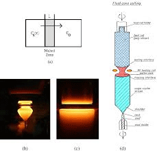 wafers. The SRI process is done through the use of water, oil or gas. When silicon is in its unrefined form, it is easily coated with a liquid suspension of ferric oxide, aluminum oxide or calcium oxide. A thin layer of wafers is created and is polished using a machine roller. This type of application is often performed in crucibles and micro-ceramic chambers.
Ultrasonic Curing - In this method, the ultrasonic sound waves are used to apply pressure to the surface of the silicon crystals. The applied pressure creates a high frequency vibration, which is translated into heat energy. The silicon is cured with the help of high temperature and pressure. This is one of the most common uses of float zone crystallization method.
Minority Carrier Lifetime - This is another important benefit of the float zone method. Silicon particles that lose their ferrous bond are deposited on the bottom of the chamber. The presence of oxygen impurities allow water to permeate into the wafers. Water then undergoes the natural liposome process. Silicon particles found on the bottom are transformed into oxygenated polymers that adsorb oxygen molecules and stops the generation of new wafers.
Detection Applications - Most common applications of float zone silicon in detector grade silicon sheets are for detection of defects on solid surface areas. The flat top surface makes it easy for the welder to transfer the material from its molds to the piece. Since the majority of welder operators use metal oxide sensors for this purpose, the low resistivity of the material is ideal for this application. However, resistivity is not the only factor that affects the process; excellent craftsmanship also plays an important role.
Applications in High-pressure Applications - There are a lot of applications for float zone silicon that require extremely low levels of light impurities. Some of them include welding, soldering, bonding, cutting, vaporizing, grinding and bonding. In most of these applications, the flat top flat surface that makes it easy for the welder to pass through is preferred. However, it has been observed that the silicon crystals grown here do not have the ability to withstand extremely high temperatures. This is one of the main reasons why manufacturers of this type of sheet prefer to grow the crystals in a stainless steel frame that can be protected from high temperatures.
Imprinting and Inspection Process - The flat top flat substrate used by manufacturers to make detector materials also helps in the inspection process. The substrate makes it easy for the inspectors to check if the components fit together or not due to the high resistivity of the material. The high resistivity is primarily affected by the impurity concentration level of the slab, but other parameters also need to be considered, like the thickness of the substrate, color, texture, and luster.
Commercialization of the float zone silicon concept has led to the production of many products. Most commonly, they are used for the creation of flat plates used in welding and soldering, which are extremely popular because of their exceptional properties. Other applications include manufacturing high-purity photoresistors, extremely effective ultra-light detectors, and flat area detectors. There are still many other uses for the high-purity crystals and several organizations are continually looking for ways to utilize this concept for their product needs.
