Get Your Quote FAST! Or, Buy Online and Start Researching Today!
What Methods are used to Grow Silicon Crystals?
The Czochralski method was first developed by Polish scientist J. Czochralski in 1916. It is still the preferred method of single crystal production. The crystals are grown by drawing them out of liquid Si. Seed crystals are dipped into the melt and withdrawn slowly at a temperature higher than the melting point. The diameter of the silicon crystal is determined by pulling rate and temperature profile. During the growth process, the growth is carried out at a controlled temperature.
![]() The seed and crucible are counter-rotated. The first part of the crystal is pushed at a fast rate, with a thin round neck. Argon is used as the growth atmosphere. The material composition of the silicon crystal depends on the method employed. Once the crystal has started growing, the preparation of the materials is important. Once the substrate has been cooled down, the crystal begins to grow. In this way, silicon is grown without any impurities.
The seed and crucible are counter-rotated. The first part of the crystal is pushed at a fast rate, with a thin round neck. Argon is used as the growth atmosphere. The material composition of the silicon crystal depends on the method employed. Once the crystal has started growing, the preparation of the materials is important. Once the substrate has been cooled down, the crystal begins to grow. In this way, silicon is grown without any impurities.
The materials used for the growth of silicon crystals must be physically compatible with the material that is to be used to grow it. A high-temperature AHP heater is recommended to reduce convexity. Once the interface is flat, the growth can be continued. In this method, faceted growth of the Si was observed, and the faceted area occupied nearly all of the cross section of the crystal. If this method can be applied to single crystal ingots, it can become a practical technology for silicon applications.
Another method of growth of silicon crystals is the process of dislocation multiplication. This method enables the growth of high-purity and uniformly doped silicon crystals. It also enables high-resistance silicon wafers up to 20 kO cm. This process is very promising, as it can be used for manufacturing semiconductors and solar cells. This method has the advantage of being extremely versatile and adaptable.
The growth of silicon crystals in this way allows the control of various chemical and electrical properties. The addition of a dopant is a process that enhances the electrical properties of the silicon crystal. It is commonly used to make transistors. In some cases, impurities may cause distortions in the semiconductor. During the growth process of silicon crystals, it is necessary to have a specialized crucible for the crystals.
Float zone crystal growth is the main method of silicon crystal growth. It is used only in some special cases and results are unreliable. The float zone method is a highly specialized method of silicon crystal growth and is still widely used. The authors have compiled an excellent volume that is worth reading. This chapter will help you understand the science behind the growth of Silicon. It is an essential text for engineers, scientists, and other professionals in the field.
The water-cooled jacket is a useful tool for controlling the heat transfer in silicon crystals. It also controls the radial temperature of the silicon crystal. In addition to the float-zone technique, it is possible to produce silicon crystals with ultra-low concentrations of carbon, oxygen, and nitrogen. In both cases, the materials are compatible and the results depend on the quality of preparation. This article covers several methods for producing semiconductors.
Float zone process is the main method of silicon crystal growth. It is an ideal method for silicon single crystals because it is easy to scale up and produces uniform-sized silicon. Its advantage is that it can be a more precise and accurate method than the float zone process. The float zone method was popular at the beginning of the Si age, but it is now only used in some special cases. There are two other methods that are widely available for the formation of single silicon.
The thermal method for silicon crystal growth has numerous advantages. The thermal process allows high-purity silicon crystals to be grown. In addition to this, it also facilitates the growth of silicon wafers with high-resistance. As a result, it is possible to produce semiconductors with high-quality, uniform, and inexpensively grown materials. This method is known as no-cutting. It can be easily modified to produce no-cut silicon.
Related Silicon Wafer Resources
- Silicon Wafers
- Silicon Ingots
- Silicon Ingot to Wafer Process
- Czochralski Silicon Growth
- Float Zone Silicon Wafers
- Silicon-on-Sapphire Wafers
- Epitaxial Silicon Wafers
How to Prepare Silicon Wafers
1. Silicon Formation
To create silicon, three crucial reactions have to be completed in sequence.
- Silicon dioxide is blended with Carbon such that they chemically react forming Silicon and carbon dioxide as the final products. The silicon formed has a percentage purity of ninety-nine percent. The equation below summarizes this first step.

- In the second step, silicon from the first step is chemically reacted with hydrogen chloride. This results in the formation of trichlorosilane and hydrogen gas as summarized by the equation below.

- The final step entails the decomposition of the formed trichlorosilane by using the resistive heating method. The decomposition occurs in a hydrogen-controlled chamber. At the end of the process, pure polycrystalline silicon rods are produced and the equation below chemically illustrates this step.

The obtained polycrystalline crystal has a purity range of 99.99999%. At this stage, we have a silicon rod that has many crystals (Merill L. Minges, 1989).
2. Growing Single-Crystalline Silicon
Two methods can be used to obtain single-crystal silicon i.e. the Czochralski method and the float zone technique. Czochralski method is used to grow single crystals on metals while the float zone method is used when high purity crystals are desired.
I. The Czochralski method
In this method, a small single crystal seed that is attached to a rod is dipped into the molten silicon. The seed is then slowly removed from the molten silicon while the rod is rotating. The figure below illustrates the process.
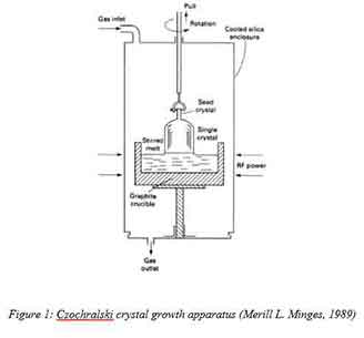 Graphite is used to make the crucible while its lining is made of fused silica. The process requires an inert atmosphere gas condition such (e.g. argon) at a pressure ranging from 0.13 – 6.7-kilo pascals. Silicon concentration is adjusted by adding highly doped silicon pellets to the melt. By constantly rotating the crystal seed, the concentration of the dopant is uniformly distributed. The rotation also does provide a uniform thermal condition as crystal growth takes place. The molten silicon has to be maintained at temperatures above 425 degrees Celsius. The melt in contact with the crystal seed solidifies as a result of a reduction in temperature. The solidification occurs at the same crystal orientation as that of the starting seed. The rod pulling rate and the melt temperatures determine the ignot diameter (Merill L. Minges, 1989). Sorting of the wafers obtained by this process is based on resistivity.
II. The Float Zone Method
For this process, a chamber having argon in controlled amounts is required. First, a polycrystalline rod is 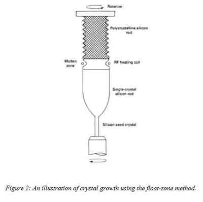 placed in the chamber. Then a single seed crystal that has a specified orientation is attached to the rod at one end. Melting as a result of the action of an induction coil that is positioned around the rod occurs and it begins with the single – seed crystal. The heating coil moves along the length of the rod causing a shift in the molten zone. When the molten silicon re-solidifies, it forms a single crystal growth with a specific orientation (Merill L. Minges, 1989). The float zone process is shown in the figure below.
This process produces single crystal silicon ignots that have high resistivity and moderate diameter values. The heating coil motion determines the crystal diameter. Typical resistivity values of produced wafers by the floating zone process varies from 25 – 30000 ohm-cm.
III. Silicon-on-Sapphire (SOS) method
The Epitaxial growth of silicon occurs on a silicon wafer, silicon-on-sapphire material is formed. This ![]() discovery was made in the year 1964. By using the Czochralski method, sapphire crystals can be obtained. The obtained sapphire is divided to form wafers which have to undergo chemical and mechanical polishing. The sapphire-based wafers then undergo hydrogen etching carried out in an epitaxial reactor at a temperature of 1150 degrees Celsius. Pyrolysis process of silane at temperatures of between 900 to 1000 degrees Celsius deposits a silicon film on the wafer. Since there exists a lattice mismatch affecting sapphire and silicon, a higher defect density exists in the silicon firm particularly in extremely thin firms though the defect appears to decrease as the thickness of the firm increases. The main defects of wafers obtained by this method are twins and stacking errors. At room temperature, the silicon firm is always under compressive stress as a result of the different thermal expansion coefficients of sapphire and silicon (Colinge, 2004).
discovery was made in the year 1964. By using the Czochralski method, sapphire crystals can be obtained. The obtained sapphire is divided to form wafers which have to undergo chemical and mechanical polishing. The sapphire-based wafers then undergo hydrogen etching carried out in an epitaxial reactor at a temperature of 1150 degrees Celsius. Pyrolysis process of silane at temperatures of between 900 to 1000 degrees Celsius deposits a silicon film on the wafer. Since there exists a lattice mismatch affecting sapphire and silicon, a higher defect density exists in the silicon firm particularly in extremely thin firms though the defect appears to decrease as the thickness of the firm increases. The main defects of wafers obtained by this method are twins and stacking errors. At room temperature, the silicon firm is always under compressive stress as a result of the different thermal expansion coefficients of sapphire and silicon (Colinge, 2004).
3. Ingot Processing
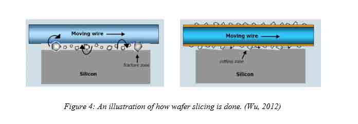
After the crystal growth procedure is done, the top and bottom ends of the ingot are cut off. The cut surface is then polished to form a flat surface that has the same diameter as the ingot. Afterward, a steel saw blade that has a diamond cutting edge divides the ingot into circular portions called wafers. For one to classify a silicon slice, one has to define the dopant used, the diameter of the substrate, the resistivity of the layer, the type of conductivity, the thickness of the slice, the orientation, surface finish quality and the flatness degree among other specifications. The numbering of the slice is from the crystal seed end to the top surface. Wafer slicing process introduces imperfections to the wafer thus necessitating for polishing. After polishing, a flat surface is obtained that aides in the photo-lithography step (Merill L. Minges, 1989). The process of polishing also reduces the thickness of the wafer that aids in proper handling without damage. The wafer has a substrate on which devices may be built.
4. Wafer- surface cleaning
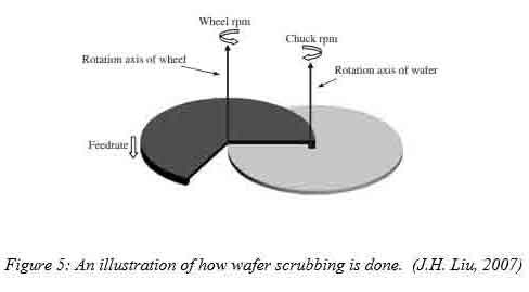 Photo-resist imaging procedure needs a clean surface thus there is a need for the removal of the surface contaminants before the process. Organic contaminants can be removed by the wet chemistry process that entails burning the material at temperatures between 900 and 1200 degrees Celsius while in an oxidation furnace. Inorganic contaminants as a result of airborne salts, storage cans, or the processing materials can be removed by absorption. Wafer scrubbing procedure may also be used to remove airborne particles contaminating the wafer surface. Scrubbing combined with chemical action will considerably remove the surface impurities (Merill L. Minges, 1989).
5. Wafer initial Probing
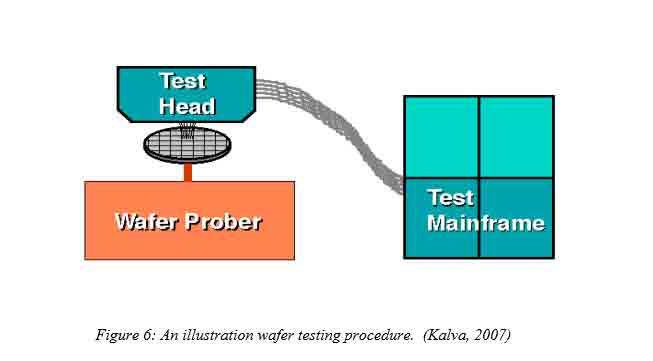
This process involves carrying out tests on the wafer to ensure that the wafer is of the desired quality before further processing. The deformities of the wafer, resistivity, doping levels at different depths plus oxide quality tests are detected in this stage. The existence of pinholes is found out to study the oxide layer (Merill L. Minges, 1989).
SOI Tech References
Colinge, J. P. (2004). Silicon-on-Insulator Technology: Materials to VLSI: Materials to Vlsi. Springer Science & Business Media .
J.H. Liu, Z. P. (2007). Grinding wheels for manufacturing of silicon wafers: A literature review. International Journal of Machine Tools & Manufacture, 1-13.
Kalva, D. (2007). WAFER PROBE AND PACKAGE TEST FAILURE ANALYSIS. All Theses.
Kirby, K. W. (2008). PROCESSING OF SAPPHIRE SURFACES FOR SEMICONDUCTOR DEVICE APPLICTIONS. Pennsylvania: The Pennsylvania State University.
Merill L. Minges. (1989). Electronic Materials Handbook: Packaging. ASM International .
Wu, H. (2012). FUNDAMENTAL INVESTIGATIONS OF CUTTING OF SILICON FOR PHOTOVOLTAIC APPLICATIONS. Georgia: Georgia Institute of Technology.
